Method for forming semiconductor structure, ldmos transistor and method for forming same

A technology of semiconductors and transistors, which is applied in the field of semiconductor manufacturing and can solve problems such as the need to improve the electrical performance of LDMOS transistors

Active Publication Date: 2021-06-08
SEMICON MFG INT (SHANGHAI) CORP +1
View PDF4 Cites 0 Cited by
  • Summary
  • Abstract
  • Description
  • Claims
  • Application Information

AI Technical Summary

Problems solved by technology

[0005] However, after the introduction of the fin field effect transistor structure, the electrical performance of the LDMOS transistor formed by the prior art still needs to be improved.

Method used


Image

  • Method for forming semiconductor structure, ldmos transistor and method for forming same
  • Method for forming semiconductor structure, ldmos transistor and method for forming same
  • Method for forming semiconductor structure, ldmos transistor and method for forming same

Examples


Embodiment Construction

[0021] It can be seen from the background art that after the fin field effect transistor structure is introduced, the electrical performance of the LDMOS transistor formed in the prior art still needs to be improved. Combining with the formation process of an LDMOS transistor, the reason why its electrical performance still needs to be improved is analyzed:

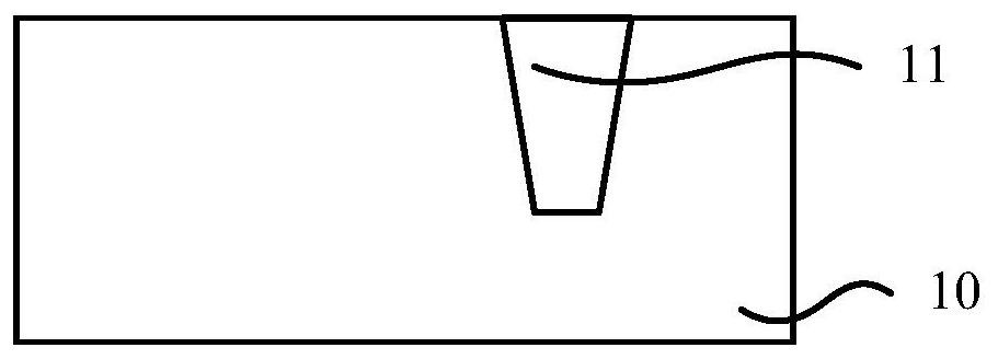
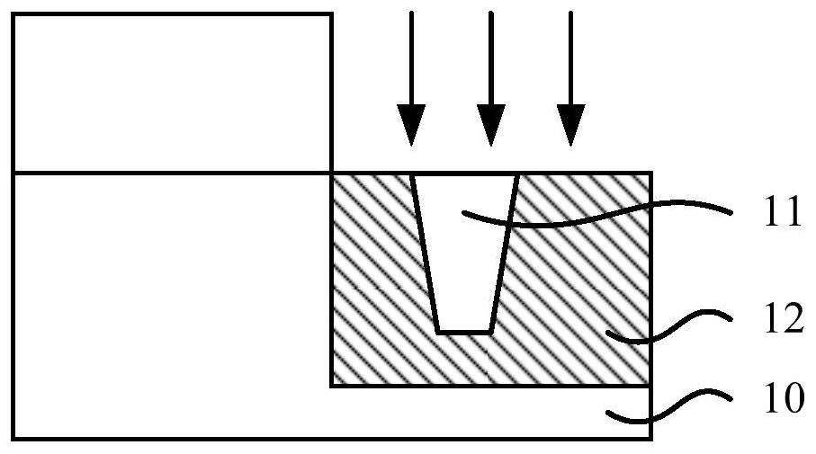
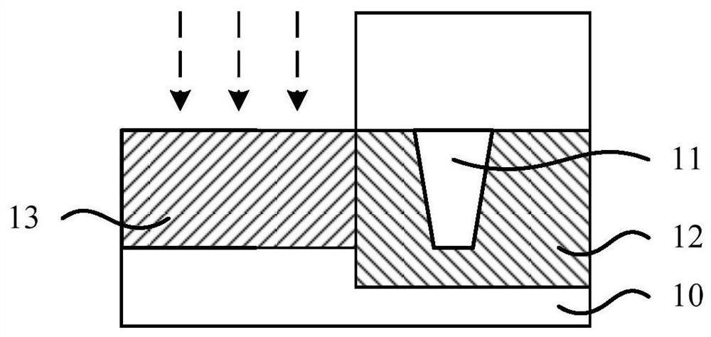
[0022] In the LDMOS transistor, there is a drift region with a lower doping concentration between the source region and the drain region, and the drift region has a higher resistance value and can withstand a higher voltage. In addition, the isolation structure is introduced into the drift region, and the gate structure covers part of the isolation structure, so as to weaken the surface electric field of the drift region, so as to improve the withstand voltage performance of the LDMOS transistor.

[0023] refer to Figure 1 to Figure 4 , shows a schematic cross-sectional structure corresponding to each step in the formati...


PUM


Abstract

A method for forming a semiconductor structure, an LDMOS transistor, and a method for forming the same. The method for forming the semiconductor structure includes: providing a base, the base including: a substrate and a fin located on the substrate; performing isolation implantation treatment, in the An isolation region is formed within the fin. The isolation region is formed by isolation implantation, so the process of forming the isolation region does not need to etch the fin, which can effectively reduce the difficulty of the formation process and will not change the surface morphology of the substrate, It can reduce the impact of the formation process of the isolation region on the subsequent process, thereby helping to reduce the process difficulty of the subsequent steps and improve the process quality of the subsequent steps; when the semiconductor structure is used to form LDMOS transistors, the technical solution of the present invention has It is beneficial to improve the process quality and to improve the electrical performance of the formed LDMOS transistor.

Description

technical field [0001] The invention relates to the field of semiconductor manufacturing, in particular to a method for forming a semiconductor structure, an LDMOS transistor and a method for forming the same. Background technique [0002] A lateral diffusion field effect (Lateral Diffusion MOS, LDMOS) transistor is a semiconductor structure that forms a lateral current path on the surface of a semiconductor substrate through planar diffusion. Compared with traditional MOS transistors, LDMOS transistors have a lightly doped region between the source region and the drain region, which is called a drift region. Therefore, when the LDMOS transistor is connected to a high voltage between the source region and the drain region, the drift region can withstand a higher voltage drop, so the LDMOS transistor can have a higher breakdown voltage. [0003] The LDMOS transistor includes a source region within a semiconductor substrate, a drain region, and a channel region between the so...

Claims


Application Information

Patent Timeline
Patent Type & Authority Patents(China)
IPC IPC(8): H01L29/06H01L29/10H01L29/78H01L21/336
CPCH01L29/063H01L29/0649H01L29/1033H01L29/66681H01L29/7816
Inventor 赵猛
Owner SEMICON MFG INT (SHANGHAI) CORP
Why Eureka
Try Eureka