Thin film transistor and preparation method thereof and thin film transistor drive backboard
A technology of thin film transistors and insulating films, which is applied in the field of metal oxide thin film transistors and their preparation, and thin film transistor drive backplanes. Deterioration and other problems, to avoid channel short circuit or decline in conductivity, low parasitic capacitance, and reduce the number of times
- Summary
- Abstract
- Description
- Claims
- Application Information
AI Technical Summary
Problems solved by technology
Method used
Image

Examples
Embodiment 1
[0086] A method for preparing a metal oxide thin film transistor that suppresses the generation of parasitic capacitance, comprising the following steps in sequence:
[0087] In step a, a metal conductive layer is deposited and patterned on the substrate as a gate metal layer.
[0088] Before step a, silicon dioxide or silicon nitride can be pre-deposited on the transparent substrate as a buffer layer.
[0089] The metal used in the metal conductive layer is aluminum, copper, molybdenum, titanium, silver, gold, tantalum, tungsten, single chromium or aluminum alloy.
[0090] The metal conductive layer is a single-layer aluminum film, copper film, molybdenum film, titanium film, silver film, gold film, tantalum film, tungsten film, chromium film or aluminum alloy film, or two or more layers composed of the above single-layer metal films film.
[0091] The thickness of the metal conductive layer is set to 100nm to 2000nm; step b is entered after step a is completed.
[0092] I...
Embodiment 2
[0118] A method for preparing a metal oxide thin film transistor that suppresses the generation of parasitic capacitance, other steps are the same as in embodiment 1, the difference is that: between process steps d and e, there is also a step y, hydrophobic to the second insulating film The second insulating film having a hydrophobic layer is obtained by the chemical treatment.
[0119] Step y is specifically: spin-coat F-series polymer Cytop on the second insulating film to obtain a hydrophobic layer, F-series polymer Cytop is perfluorinated polymer Cytop or fluorocarbon polymer Cytop or AF cyclized fluorine At least one of the carbon polymer Cytop, the thickness of the hydrophobic layer is 5-20nm.
[0120] The preparation process of the thin film transistor of the present invention uses a self-alignment method to make an etching barrier layer, which maintains the structural characteristics of the bottom gate and the etching barrier layer, and can ensure the stability of the ...
Embodiment 3
[0125] A method for preparing a metal oxide thin film transistor that suppresses the generation of parasitic capacitance, comprising the following steps in sequence:
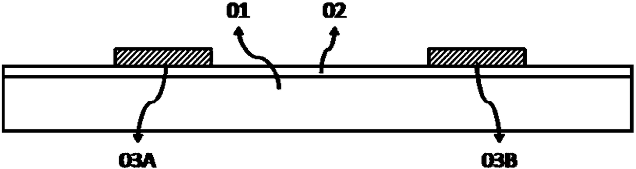
[0126] Such as figure 1 shown, in a SiO with 200nm thick 2 On the non-alkali glass substrate 01 of the buffer layer 02, a three-layer Mo / Al / Mo metal thin film is sequentially deposited by PVD (Physical Vapor Deposition) method, with thicknesses of 25nm / 100nm / 25nm respectively. It is patterned using a photolithography process to form a gate metal layer 03 .
[0127] It should be noted that the thickness of the gate metal layer is in the range of 100 nm to 2000 nm, and its specific size can be flexibly set according to actual needs, and is not limited to the size of this embodiment. The constituent material of the gate metal layer is also not limited to the case of this embodiment.
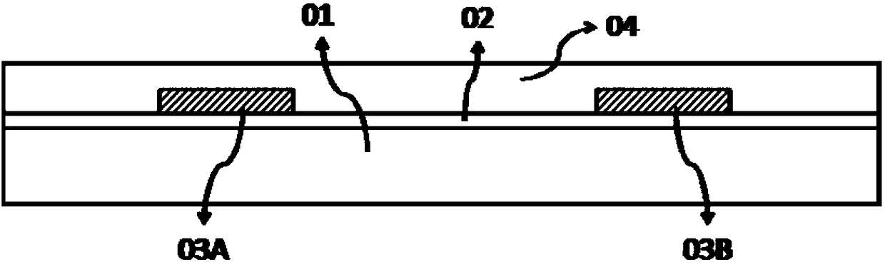
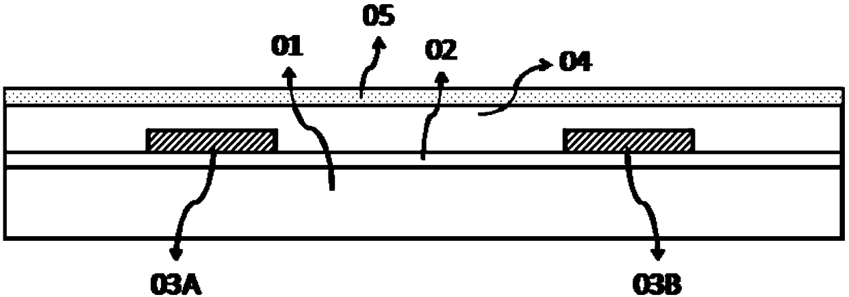
[0128] Such as figure 2 As shown, on the patterned gate metal layer 03, the PECVD method (Plasma Enhanced Chemical Vapor Depos...
PUM
| Property | Measurement | Unit |
|---|---|---|
| electrical resistivity | aaaaa | aaaaa |
| thickness | aaaaa | aaaaa |
| thickness | aaaaa | aaaaa |
Abstract
Description
Claims
Application Information
 - R&D
- Intellectual Property
- Life Sciences
- Materials
- Tech Scout
- Unparalleled Data Quality
- Higher Quality Content
- 60% Fewer Hallucinations
Browse by: Latest US Patents, China's latest patents, Technical Efficacy Thesaurus, Application Domain, Technology Topic, Popular Technical Reports.
© 2025 PatSnap. All rights reserved.Legal|Privacy policy|Modern Slavery Act Transparency Statement|Sitemap|About US| Contact US: help@patsnap.com