Soldering-resistant printing method of circuit board

A circuit board and solder mask technology, which is applied in the fields of printed circuit manufacturing, printed circuit, and secondary treatment of printed circuit, etc., can solve problems such as redness of circuit, side erosion of green oil bridge, difficult production, etc., and achieve reduction of hole area ink effect

Active Publication Date: 2018-05-08
HUIZHOU TECHUANG ELECTRONIC TECH CO LTD
View PDF6 Cites 11 Cited by
  • Summary
  • Abstract
  • Description
  • Claims
  • Application Information

AI Technical Summary

Problems solved by technology

[0002] With the development of the industry, whether it is functionality or appearance, enterprises have higher and higher requirements for products. Generally, customers' requirements for the appearance of circuit boards are mainly the effect of solder mask printing. According to the characteristics of solder mask ink, the ink is printed on the circuit board. The ink will spread out when the ink is on the line, and the thickness of the ink on the line is generally thinner than that on the plane. The thicker the copper thickness, the more difficult it is to make, and there are quality risks such as redness of the line (false exposed copper), side erosion of green oil bridges, and golden holes.

Method used


Image

  • Soldering-resistant printing method of circuit board
  • Soldering-resistant printing method of circuit board
  • Soldering-resistant printing method of circuit board

Examples


Embodiment

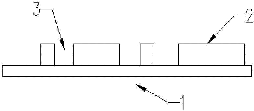
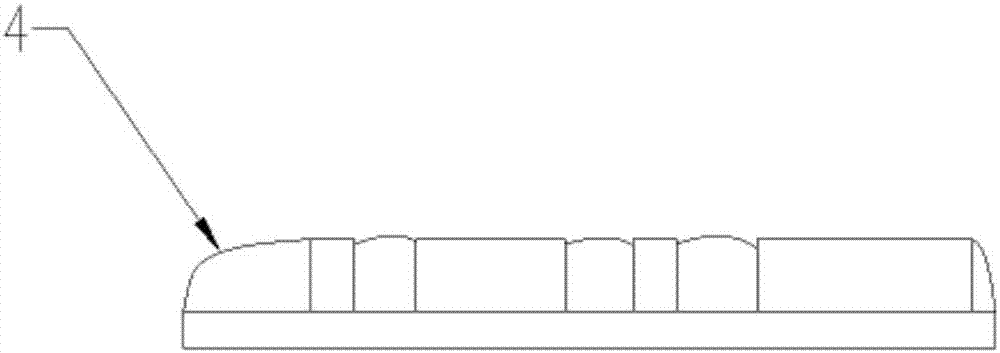
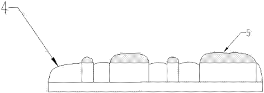
[0033] Solder mask printing is to transfer the ink to the circuit board through the method of screen leakage to form a pattern consistent with the negative. The solder mask is a protective film that prevents bridging during soldering and provides a long-term insulation environment and Anti-chemical protection, forming a beautiful coat of PCB board. In resist printing, green oil, that is, liquid photo solder resist is usually used.

[0034] The specific functions of solder mask printing are as follows:

[0035] A. Solder protection: Leave the through holes and PAD on the board to cover all the circuits and copper surfaces to prevent short circuits during wave soldering and save the amount of solder;

[0036] B. Protective board: prevent the corrosion of moisture, acid-base environment and various electrolytes from oxidizing the circuit and causing electrical performance problems, and prevent external mechanical damage to maintain the insulation effect of the circuit board;

[0037] C....


PUM


Abstract

The invention discloses a soldering-resistant printing method of a circuit board. The soldering-resistant printing method comprises the following steps of S1, pre-treatment; S2, paraffin loading, in which liquid-state paraffin is uniformly coated on a non-circuit region of a panel by a silk-screen printing or curtain coating mode, and the liquid-state paraffin is cured on the non-circuit region ofthe panel; S3, soldering-resistant printing, in which oil is coated on a circuit by employing a circuit net plate; S4, pre-baking; S5, exposure and alignment; S6, paraffin removal, in which a circuitboard with ink hardened and attached onto panel is placed in hot water to remove the paraffin; S7, baking; S8, soldering-resistant printing again, in which the ink is uniformly coated on the whole panel of the circuit board by employing the net plate of the whole panel; and S9, post-baking. According to the soldering-resistant printing method disclosed by the invention, the ink thickness of a circuit position is ensured by a mode of changing printing, meanwhile, the ink on a plane is not too thick, the risks of ink accumulated in a hole and green oil bridge lateral erosion are reduced, and the requirement of soldering-resistant quality of a thick-copper circuit board is met.

Description

Technical field [0001] The invention relates to the technical field of printed circuit boards, in particular to a circuit board solder resist printing method. Background technique [0002] With the development of the industry, whether it is functionality or appearance, companies have higher and higher requirements for products. The general customer’s requirements for the appearance of circuit boards are mainly the effect of solder mask printing. According to the characteristics of solder mask ink, the ink is printed on the line The ink will diverge, and the thickness of the ink on the line is generally thinner than that on the plane. The thicker the copper, the more difficult it is to make, and there are quality risks such as redness of the line (false exposed copper), side erosion of green oil bridges, and golden holes. . Summary of the invention [0003] The purpose of the present invention is to solve the above-mentioned shortcomings in the prior art and provide a solder mask ...

Claims


Application Information

Patent Timeline
Patent Type & Authority Applications(China)
IPC IPC(8): H05K3/28
CPCH05K3/282H05K2203/1377
Inventor 许校彬陈金星董恩佳祝剑陈义仁
Owner HUIZHOU TECHUANG ELECTRONIC TECH CO LTD
Why Eureka
Try Eureka