Method for manufacturing metal laser melting additive
A technology of laser melting additive and manufacturing method, which is applied in the field of additive manufacturing to achieve the effects of low comprehensive production cost, high dense structure and high part qualification rate
- Summary
- Abstract
- Description
- Claims
- Application Information
AI Technical Summary
Problems solved by technology
Method used
Image


Examples
Embodiment 1
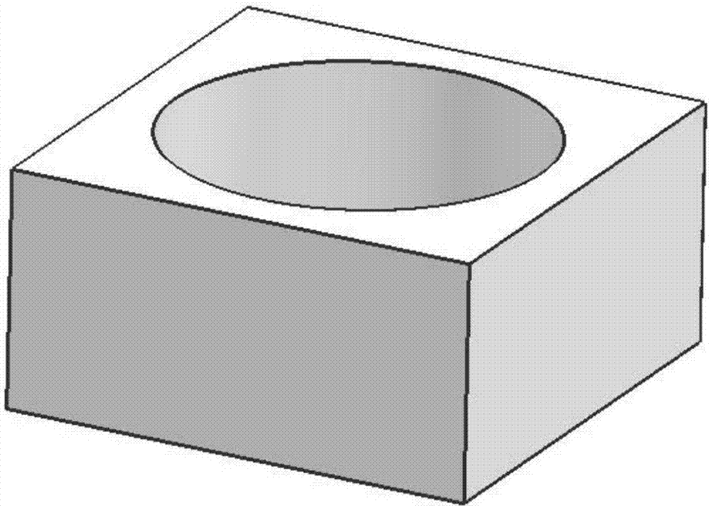
[0031] (1) For the forming of high-performance 316L stainless steel alloy parts, the three-dimensional CAD model of the part is designed by using three-dimensional modeling software ( figure 1 ), and then processed by the slicing software and saved as an STL file ( figure 2 ), the data information of the STL file is sent to the laser additive manufacturing rapid prototyping equipment; the current slice layer is processed by the selective laser melting method, and the powder feeding mechanism spreads a layer on the metal substrate with a thickness of about 0.02mm and a particle size of 10μm 316L stainless steel powder, fiber laser power 160W; image 3 Laser scan the trajectory for the current layer to be printed.
[0032] (2) After processing the current slice layer, use an ultrasonic probe to scan the laser melting area line by line. Record the position of the defect feature, and set the rounded rectangle containing the defect ( Figure 4 ). After the flaw detection is co...
Embodiment 2
[0036] (1) For the forming of high-performance cobalt-based Co-27Cr-5Mo-0.5Ti alloy parts, use 3D modeling software to design the 3D CAD model of the part, and then save it as an STL file after being processed by the slicing software, and the data information of the STL file Delivered to laser additive manufacturing rapid prototyping equipment; the current slice layer is processed by laser near-net forming technology, so that 500W YAG laser, 50g / min cobalt-based alloy powder, and Ar gas are input to the substrate at the same time, with a layer thickness of 0.1mm;
[0037] (2) After processing the current slice layer, use an ultrasonic probe to scan the laser melting area line by line. Record the location of the defect feature, and set the enclosing rounded rectangle. After the flaw detection is completed, replace the ultrasonic probe with a milling cutter, and cut off the rounded rectangular area with a cutting thickness of 0.1mm;
[0038] (3) Re-use the laser near-net shapin...
PUM
| Property | Measurement | Unit |
|---|---|---|
| particle diameter | aaaaa | aaaaa |
Abstract
Description
Claims
Application Information
 - R&D
- Intellectual Property
- Life Sciences
- Materials
- Tech Scout
- Unparalleled Data Quality
- Higher Quality Content
- 60% Fewer Hallucinations
Browse by: Latest US Patents, China's latest patents, Technical Efficacy Thesaurus, Application Domain, Technology Topic, Popular Technical Reports.
© 2025 PatSnap. All rights reserved.Legal|Privacy policy|Modern Slavery Act Transparency Statement|Sitemap|About US| Contact US: help@patsnap.com