


Quick Research
Generate reliable direction feasibility study reports for your R&D in just a few steps.

Technical Q&A
Discover and master advanced knowledge NOW. Basics, ideas, possibilities, all at once.

Find Solutions
As an expert in R&D theories, this can generate solutions to your technical problems instantly.

Evaluate Feasibility
Analyze your overall solution with one click, know your potential R&D risks in advance.

Monitor Landscape
Get weekly tech updates, stay abreast of the latest tech innovations and key insights.
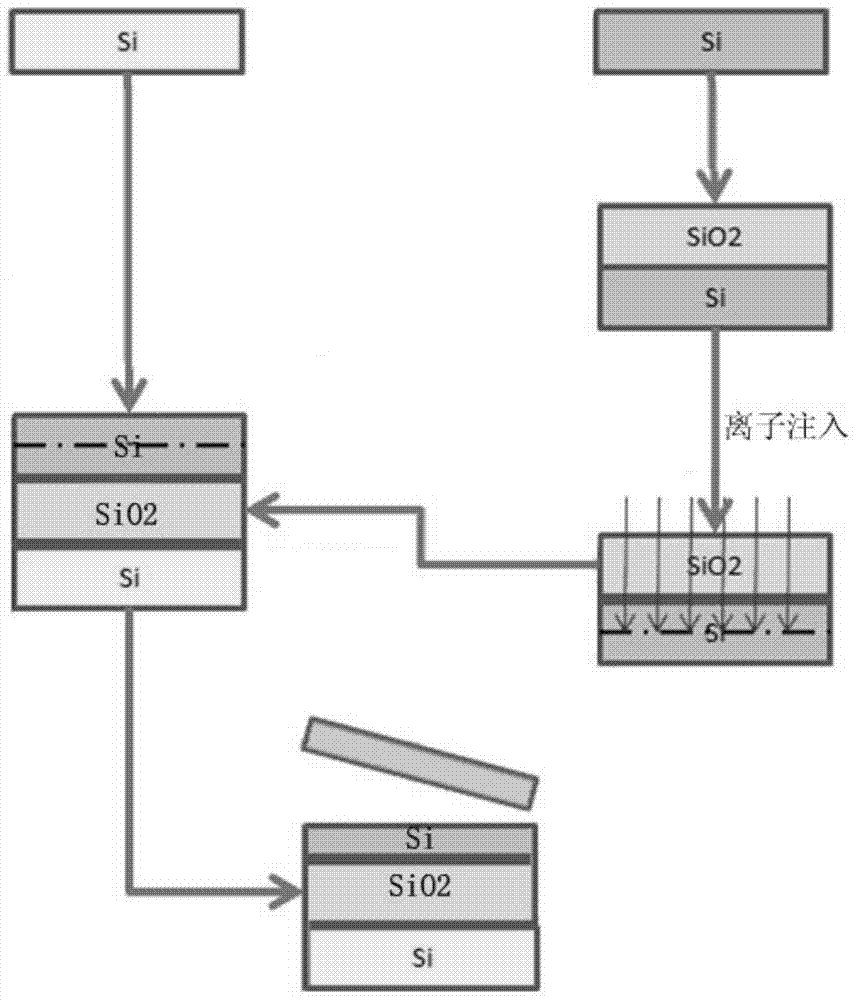
Method for preparing SOI silicon chip by means of laser chip breaking technology
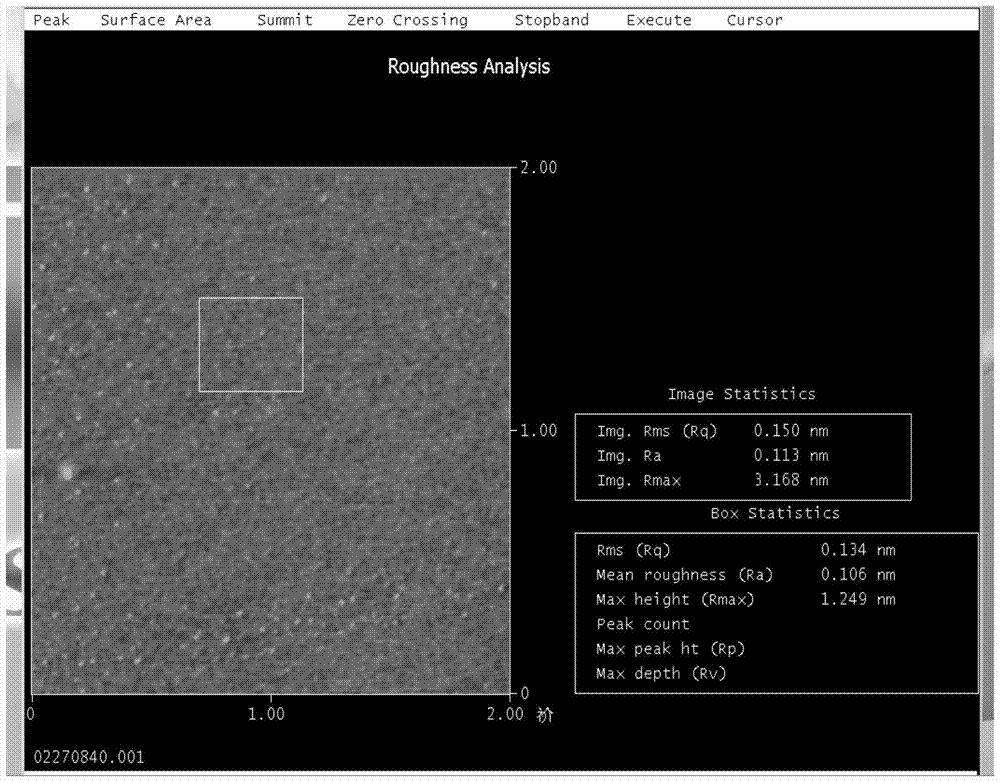
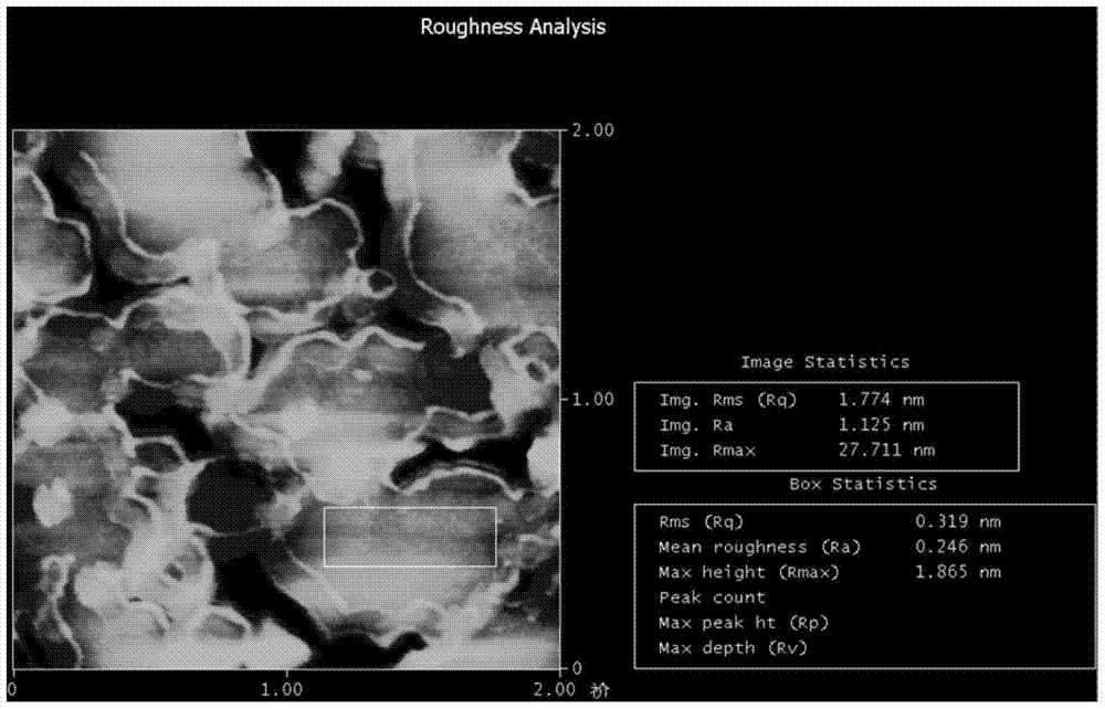
A technology of silicon wafers and splits, which is applied in the field of preparing SOI silicon wafers by using laser splitting technology, which can solve the problems that the temperature cannot be controlled and adjusted, and cannot be industrialized, so as to eliminate lattice defects, improve surface roughness, and remove surface adsorption substances. Effect
- Summary
- Abstract
- Description
- Claims
- Application Information
AI Technical Summary
Problems solved by technology
Method used
Image

Examples
Embodiment 1
[0024] 1. Take an 8-inch P-type silicon wafer, its crystal orientation can be selected from or , and its resistivity can be selected from light doping to high resistance.
[0025] 2. Preparation of oxide layer (silicon dioxide) on the silicon wafer: oxidize one surface of the silicon wafer in step 1 (or both wafers can be oxidized, according to the actual process conditions) to obtain a silicon wafer with an oxide layer (Silicon dioxide is used as the BOX layer of SOI), the oxidation adopts a conventional process, and the thickness of the prepared oxide layer (silicon oxide) is >0-1000nm; the prepared silicon wafer with an oxide layer is cleaned with SC1 and SC2 in turn to remove the silicon wafer Surface contamination, and then use the test equipment to test the surface particles of the silicon wafer, use the test equipment to test the thickness of the silicon oxide and other parameters (such as the particles of the silicon oxide layer, electrical parameters), select the sili...
PUM
| Property | Measurement | Unit |
|---|---|---|
| Thickness | aaaaa | aaaaa |
Abstract
Description
Claims
Application Information
 - R&D Engineer
- R&D Manager
- IP Professional
- Industry Leading Data Capabilities
- Powerful AI technology
- Patent DNA Extraction
Browse by: Latest US Patents, China's latest patents, Technical Efficacy Thesaurus, Application Domain, Technology Topic, Popular Technical Reports.
© 2024 PatSnap. All rights reserved.Legal|Privacy policy|Modern Slavery Act Transparency Statement|Sitemap|About US| Contact US: help@patsnap.com