
Metal housing used for semiconductor power device

A technology of power devices and metal casings, applied in the field of new power semiconductor devices, can solve problems such as large internal space, and achieve the effects of low cost, reduced attenuation, and reduced trending effect.

Inactive Publication Date: 2017-07-18
宜兴市吉泰电子有限公司
View PDF4 Cites 2 Cited by
  • Summary
  • Abstract
  • Description
  • Claims
  • Application Information

AI Technical Summary

Problems solved by technology

Due to the small size of the chip carrying the metal-oxide semiconductor field effect transistor, the small size of the shell but the large internal space, and the need for heat dissipation and the role of ensuring that the electromagnetic signal generated by the internal circuit does not affect the external circuit, the current existing technology is very It is difficult to achieve a package with good heat dissipation performance and strong shielding performance

Method used


Image

  • Metal housing used for semiconductor power device
  • Metal housing used for semiconductor power device

Examples


Embodiment Construction

[0014] The specific embodiment of the present invention will be described with reference to the accompanying drawings.

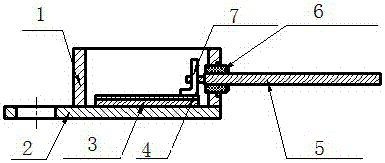
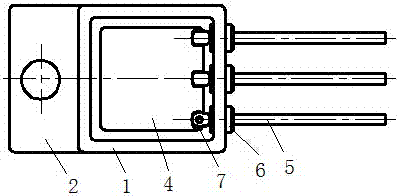
[0015] Such as figure 1 with figure 2 As shown, a metal case for a semiconductor power device, including a socket and a lead;

[0016] The tube base includes a frame-shaped steel shell 1, the bottom of the steel shell 1 has a tungsten-copper base plate 2, one end of the tungsten-copper base plate 2 extends outside the steel shell 1, and a through hole is opened on the extended part. Inside the steel shell 1, the tungsten copper bottom plate 1 is provided with a beryllium oxide sheet 3, and the beryllium oxide sheet 3 is provided with a molybdenum sheet 4;

[0017] There are three sealing holes on the steel shell 1, and lead wires 5 are respectively arranged in the three sealing holes, and the lead wires 5 and the sealing holes are connected by insulators 6; the two ends of the lead wires 5 are respectively the inner end and the outer The outer end is loc...


PUM


Abstract

The invention relates to a novel power semiconductor device, especially relates to a metal housing used for a semiconductor power device. A bottom part of a steel housing is provided with a tungsten copper bottom plate, one end of which is extended out of the steel housing, and the extended part is provided with a through hole. In the steel housing, the tungsten copper bottom plate is provided with a beryllium oxide sheet, which is provided with a molybdenum sheet. The steel housing is provided with three sealing holes, in which are disposed leads, and the leads and the sealing holes are connected together by insulators. The two ends of each lead are respectively an inner end and an outer end, and the outer end is disposed on the outer part of the steel housing, and the inner end is disposed in the steel housing, and in addition, the inner end adopts a flat structure, and the width of the inner end is greater than the diameter of the corresponding sealing hole. The inner end of one of the leads is provided with a connecting hole, in which is fixedly disposed a binding post, and the binding post is connected with the molybdenum sheet. The performance of the housing is enhanced, and the metal housing is suitable for the packaging of the large-current, high-power, high-back pressure high heat conduction semiconductor devices.

Description

technical field [0001] The invention relates to a novel power semiconductor device, in particular to a metal casing for a semiconductor power device. Background technique [0002] In the technology of controlling switches by analog circuits and digital circuits, metal-oxide semiconductor field effect transistors are usually used as electrical signals for control. In order to introduce the chip of the transistor into the circuit system, it is necessary to provide a specific package. [0003] At present, the main functions of the packaging shell of power management integrated circuit devices are: mechanical support, sealing protection, electrical signal connection, signal shielding, and heat dissipation, especially in the two elements of heat dissipation and electromagnetic signal shielding. Due to the small size of the chip carrying the metal-oxide semiconductor field effect transistor, the small size of the shell but the large internal space, and the need for heat dissipati...

Claims


Application Information

Patent Timeline
Patent Type & Authority Applications(China)
IPC IPC(8): H01L23/043H01L23/06
CPCH01L23/043H01L23/06
Inventor 孟令平何晟
Owner 宜兴市吉泰电子有限公司
Learn More