


Quick Research
Generate reliable direction feasibility study reports for your R&D in just a few steps.

Technical Q&A
Discover and master advanced knowledge NOW. Basics, ideas, possibilities, all at once.

Find Solutions
As an expert in R&D theories, this can generate solutions to your technical problems instantly.

Evaluate Feasibility
Analyze your overall solution with one click, know your potential R&D risks in advance.

Monitor Landscape
Get weekly tech updates, stay abreast of the latest tech innovations and key insights.
Compound semiconductor corrosion method
A compound and semiconductor technology, used in semiconductor/solid-state device manufacturing, electrical components, circuits, etc., can solve the problems of slow etching rate, time-consuming and energy-consuming oxidation process, inability to achieve partial etching, etc., to reduce roughness , the effect of precise control of etching rate and depth
- Summary
- Abstract
- Description
- Claims
- Application Information
AI Technical Summary
Problems solved by technology
Method used
Image


Examples
Embodiment 1
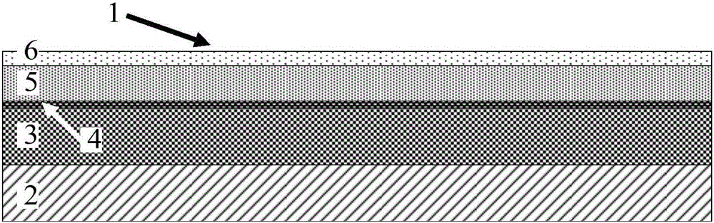
[0060] A kind of epitaxial wafer 1, the schematic diagram of its section structure is as figure 1 shown. The epitaxial wafer 1 includes a substrate 2 (sapphire substrate), a GaN buffer layer 3 (channel layer), a two-dimensional electron gas layer 4, an AlGaN barrier layer 5 (where the content of Al is adjustable) and a GaN buffer layer 5 from bottom to top. Layer 6.
[0061] The epitaxial wafer 1 is etched, and the etching method includes the following steps:
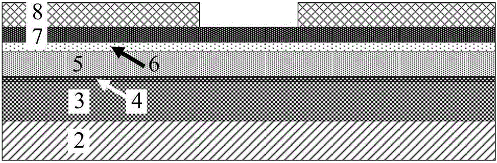
[0062] (1) Covering the mask layer 7 on the surface of the GaN layer 6, the material of the mask layer is selected from silicon oxide;
[0063] (2) Cover the photoresist layer on the surface of the mask layer 7, and obtain a patterned photoresist layer 8 by using a photolithography process;
[0064] (3) Obtaining a patterned mask layer by wet etching and / or dry etching;
[0065] (4) removing the patterned photoresist layer 8;
[0066] (5) Oxygen plasma generated by inductively coupled plasma-reactive ion etching sy...
Embodiment 2
[0081] An epitaxial wafer 1, which includes a substrate 2 (sapphire substrate), a GaN buffer layer 3 (channel layer), a two-dimensional electron gas layer 4 and an AlGaN barrier layer 5 from bottom to top.
[0082] The epitaxial wafer 1 is etched, and the etching method includes the following steps:
[0083] (1) covering the mask layer 7 on the surface of the AlGaN barrier layer 5, the material of the mask layer is selected from silicon nitride;
[0084] (2) Cover the photoresist layer on the surface of the mask layer 7, and obtain a patterned photoresist layer 8 by using a photolithography process;
[0085] (3) Obtain a patterned mask layer 7 by wet etching and / or dry etching;
[0086] (4) removing the patterned photoresist layer 8;
[0087] (5) Oxygen plasma generated by an inductively coupled plasma-reactive ion etching system is used to oxidize the exposed AlGaN barrier layer 5 to obtain an oxide layer 9, wherein, in the inductively coupled plasma-reactive ion etching sy...
Embodiment 3
[0091] A kind of epitaxial wafer 1, the schematic diagram of its section structure is as figure 1 shown. The epitaxial wafer 1 sequentially includes a substrate 2 (sapphire substrate), a GaN buffer layer 3, a two-dimensional electron gas layer 4, an AlGaN barrier layer 5 and a GaN capping layer from bottom to top.
[0092] The epitaxial wafer 1 is etched, and the etching method includes the following steps:
[0093] (1) covering the mask layer 7 on the surface of the GaN layer 6, the material of the mask layer is selected from aluminum;
[0094] (2) Cover the photoresist layer on the surface of the mask layer 7, and obtain a patterned photoresist layer 8 by using a photolithography process;
[0095] (3) Obtain a patterned mask layer 7 by wet etching and / or dry etching;
[0096] (4) removing the patterned photoresist layer 8;
[0097] (5) Oxygen plasma generated by inductively coupled plasma-reactive ion etching system is used to oxidize the exposed GaN layer 6 to obtain ox...
PUM
| Property | Measurement | Unit |
|---|---|---|
| thickness | aaaaa | aaaaa |
| thickness | aaaaa | aaaaa |
| depth | aaaaa | aaaaa |
Abstract
Description
Claims
Application Information
 - R&D Engineer
- R&D Manager
- IP Professional
- Industry Leading Data Capabilities
- Powerful AI technology
- Patent DNA Extraction
Browse by: Latest US Patents, China's latest patents, Technical Efficacy Thesaurus, Application Domain, Technology Topic, Popular Technical Reports.
© 2024 PatSnap. All rights reserved.Legal|Privacy policy|Modern Slavery Act Transparency Statement|Sitemap|About US| Contact US: help@patsnap.com