Fabrication method of wafer-level uniaxial strained SiGe on SiN buried insulating layer based on silicon nitride stress film and scale effect

A scale effect and technology on the insulating layer, applied in the field of microelectronics, can solve problems such as poor process compatibility, small strain, and poor reliability, and achieve the effects of low cost, large strain, and high reliability

Active Publication Date: 2018-11-16
XIDIAN UNIV
View PDF6 Cites 0 Cited by
  • Summary
  • Abstract
  • Description
  • Claims
  • Application Information

AI Technical Summary

Problems solved by technology

[0011] However, this method has the following disadvantages: 1) Poor compatibility with traditional integrated circuit technology: In order to obtain SGOIs with different strains, this method needs to make additional bending tables with different curvature radii, and the manufactured bending tables need to be compatible with existing With annealing equipment
2) Poor reliability: This process requires the use of pressure rods to apply mechanical force to bend the SGOI wafer, which will introduce defects into the top-layer SiGe; if the SGOI wafer bends too much, it will cause wafer fragmentation
3) Due to the fear of SGOI wafer breakage, the bending degree of mechanical bending cannot be too large, which limits the amount of strain introduced in the top SiGe, and the amount of strain that can be achieved is small

Method used


Image

  • Fabrication method of wafer-level uniaxial strained SiGe on SiN buried insulating layer based on silicon nitride stress film and scale effect
  • Fabrication method of wafer-level uniaxial strained SiGe on SiN buried insulating layer based on silicon nitride stress film and scale effect
  • Fabrication method of wafer-level uniaxial strained SiGe on SiN buried insulating layer based on silicon nitride stress film and scale effect

Examples


Embodiment 1

[0036] Example 1, preparing a 5-inch SiN buried insulating layer uniaxially strained SGOI wafer material.

[0037] Step 1: Clean the SiN buried insulating layer SGOI wafer to remove surface contaminants.

[0038] (1.1) Use acetone and isopropanol to alternately perform ultrasonic cleaning on the SGOI wafer to remove organic contamination on the substrate surface;

[0039] (1.2) Prepare a 1:1:3 mixed solution of ammonia, hydrogen peroxide, and deionized water, and heat it to 120°C, soak the SGOI wafer in the mixed solution for 12 minutes, take it out and rinse it with a large amount of deionized water, To remove inorganic pollutants on the surface of SGOI wafers;

[0040] (1.3) Soak the SGOI wafer in HF acid buffer for 2 minutes to remove the oxide layer on the surface.

[0041] Step 2: Ion implantation.

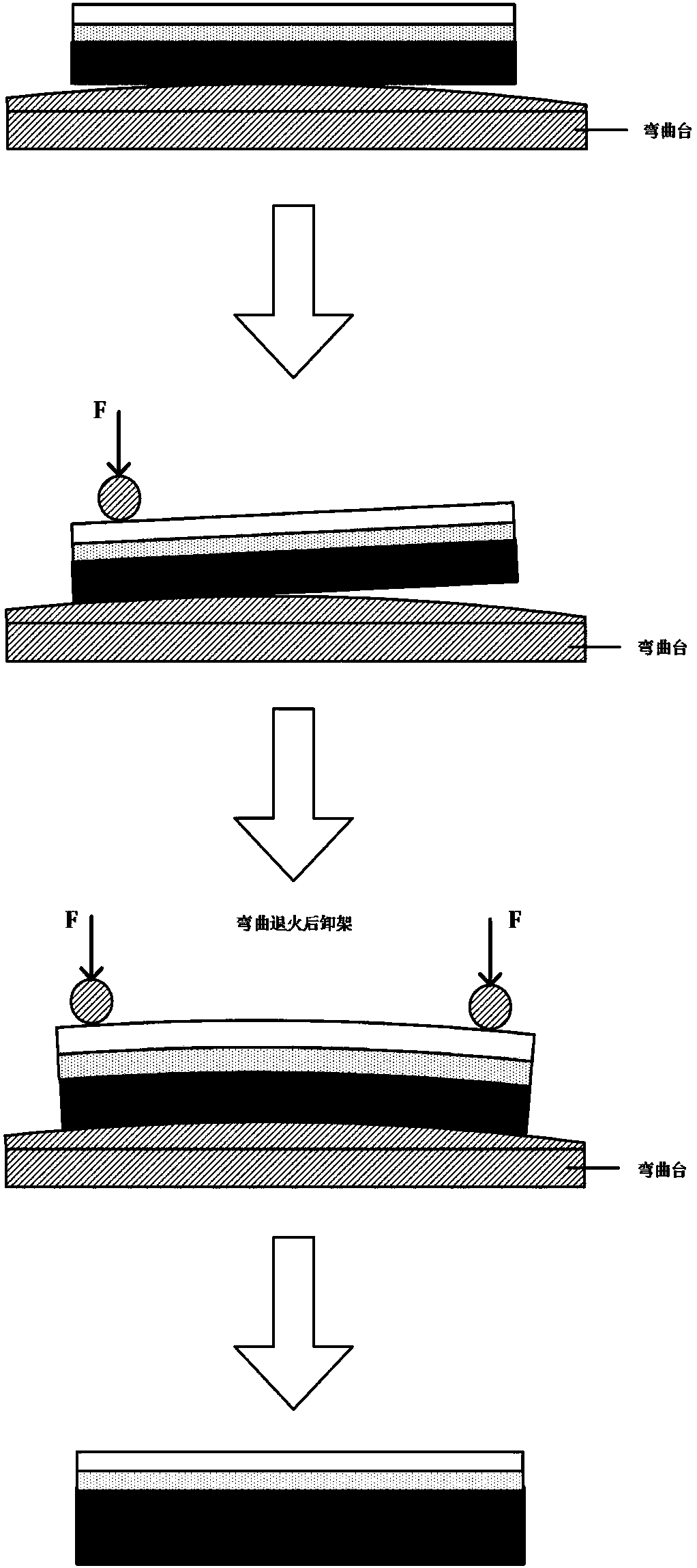
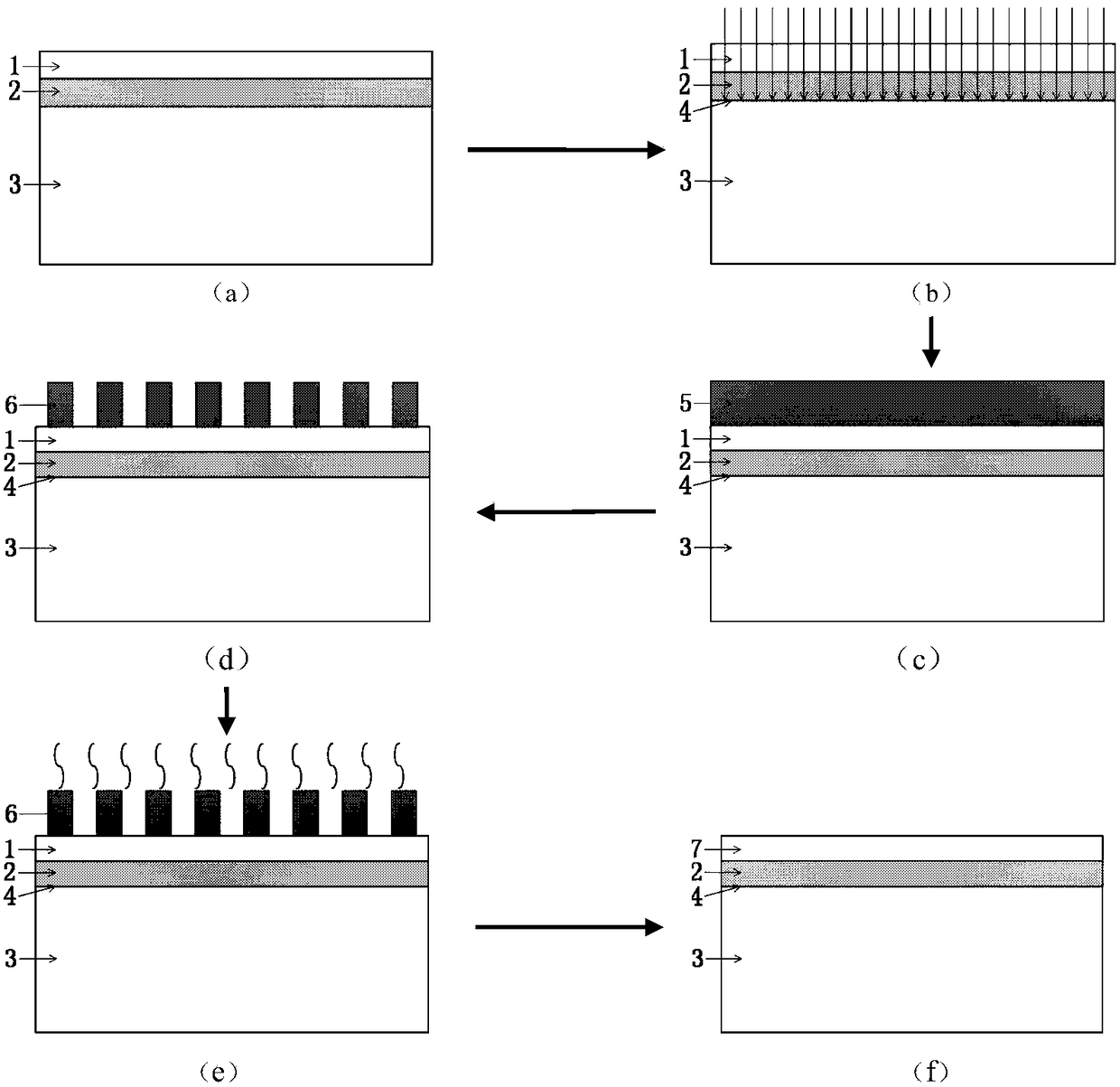
[0042] The implantation dose to the cleaned SGOI wafer is 1E14cm -2 , He ions with an energy of 50Kev to loosen the interface 4 between the Si substrate 3 and the SiN bur...

Embodiment 2

[0056] Example 2, preparing an 8-inch SiN buried insulating layer uniaxially compressively strained SGOI wafer material.

[0057] Step 1: cleaning the SiN buried insulating layer SGOI wafer to remove surface pollutants.

[0058] The implementation of this step is the same as step 1 of Embodiment 1.

[0059] Step 2: Implant the cleaned SGOI wafer with a dose of 1E15cm -2 , He ions with an energy of 85Kev to loosen the interface 4 between the Si substrate 3 and the SiN buried insulating layer 2, such as figure 2 as shown in b.

[0060] Step 3: Deposit a tensile stress SiN film 5 with a thickness of 0.7 μm and a stress of 1.2 GPa on the surface of the top SiGe layer 1 of the ion-implanted SGOI wafer, such as figure 2 as shown in c.

[0061] The realization process of this step is identical with the step 3 of embodiment 1, and its process parameter is as follows:

[0062] The reaction chamber temperature is 400°C, the reaction chamber pressure is 3.1Torr, the high frequency...

Embodiment 3

[0070] Example 3, preparing a 12-inch SiN buried insulating layer uniaxially strained SGOI wafer material.

[0071] Step A: cleaning the SiN buried insulating layer SGOI wafer to remove surface pollutants.

[0072] The implementation of this step is the same as step 1 of Embodiment 1.

[0073] Step B: Perform ion implantation on the cleaned SGOI wafer to loosen the interface 4 between the Si substrate 3 and the SiN buried insulating layer 2, such as figure 2 as shown in b.

[0074] The ion implantation process is: the implanted ions are He ions, and the implantation dose is 1E16cm -2 , inject energy 120Kev.

[0075] Step C: Depositing a SiN film.

[0076] On the surface of the top SiGe layer 1 of the ion-implanted SGOI wafer, a compressive stress SiN film 5 with a thickness of 0.9 μm and a stress of -1.3 GPa is deposited, such as figure 2 as shown in c;

[0077] The realization process of this step is identical with the step 3 of embodiment 1, and its process parameter...


PUM

PropertyMeasurementUnit
thicknessaaaaaaaaaa
widthaaaaaaaaaa
widthaaaaaaaaaa

Abstract

The invention discloses a fabrication method for wafer-level mono-axial strain SiGe on a SiN-buried insulation layer based on a silicon nitride stress thin film and a scale effect. The fabrication method is implemented according to the following steps of cleaning a silicon germanium on insulator (SGOI) wafer and performing He ion injection; depositing a press stress SiN thin film of over (-1.2)GPa or a tensile stress SiN thin film of 1.2GPa on a SiGe layer at a top layer of the SGOI wafer after ion injection, and etching the SiN thin film to form a strip-shaped array; annealing the SGOI wafer with the SiN thin film array; removing the SiN thin film array on the surface of the SGOI wafer through corrosion to obtain the wafer-level mono-axial strain SGOI material. Strain is introduced to the Ge layer at the top layer by means of mono-axial stretching or mono-axial compression plastic deformation of the SiN-buried insulation layer under the effect of the strip-shaped SiN thin film array, and the SGOI wafer needed by an integrated circuit with high temperature, high power and radiation resistance can be fabricated.

Description

technical field [0001] The invention belongs to the field of microelectronics technology, and relates to a semiconductor substrate material manufacturing process technology, specifically a method for manufacturing a wafer-level uniaxially strained SiGe material on a SiN buried insulating layer, which can be manufactured for high temperature, high power consumption, SGOI wafers required for high-power, radiation-hardened integrated circuits. Background technique [0002] As known in the industry, SiGe has the advantages of both Si and Ge, and has many advantages such as high operating frequency of devices and circuits, low power consumption, cheaper than GaAs, compatibility with Si CMOS technology, and low cost. It is widely used in microwave devices, mobile communications , high-frequency circuits and other industrial fields have broad application prospects and competitive advantages. SiGe is also an excellent optoelectronic material, and has a wide range of applications in...

Claims


Application Information

Patent Timeline
Patent Type & Authority Patents(China)
IPC IPC(8): H01L21/762H01L21/265H01L21/324
CPCH01L21/265H01L21/324H01L21/7624
Inventor 苗东铭戴显英郝跃焦帅祁林林梁彬
Owner XIDIAN UNIV
Why Eureka
Try Eureka