Growing method for light-emitting composite layer, and LED epitaxial structure comprising light-emitting composite layer
A growth method and epitaxial structure technology, applied in electrical components, circuits, semiconductor devices, etc., can solve the problems of brightness and anti-static ability not meeting the actual needs, the decline of crystal quality in the light-emitting area, and low anti-static ability, etc. Lattice defects, enhanced confinement, and improved antistatic ability
- Summary
- Abstract
- Description
- Claims
- Application Information
AI Technical Summary
Problems solved by technology
Method used
Image
Examples
Embodiment 1
[0061] Aixtron MOCVD is used to grow high-brightness GaN-based LED epitaxial wafers, specifically: high-purity H 2 or high purity N 2 or high purity H 2 and high purity N 2 The mixed gas as the carrier gas, high-purity NH 3 As the N source, the metal-organic source trimethylgallium (TMGa) is used as the gallium source, triethylgallium (TEGa) is used as the gallium source, trimethylindium (TMIn) is used as the indium source, and the N-type dopant is silane (SiH 4 ), trimethylaluminum (TMAl) as the aluminum source, and the P-type dopant as magnesium dicene (CP 2 Mg), the substrate is sapphire, and the reaction pressure is between 100mbar and 800mbar.
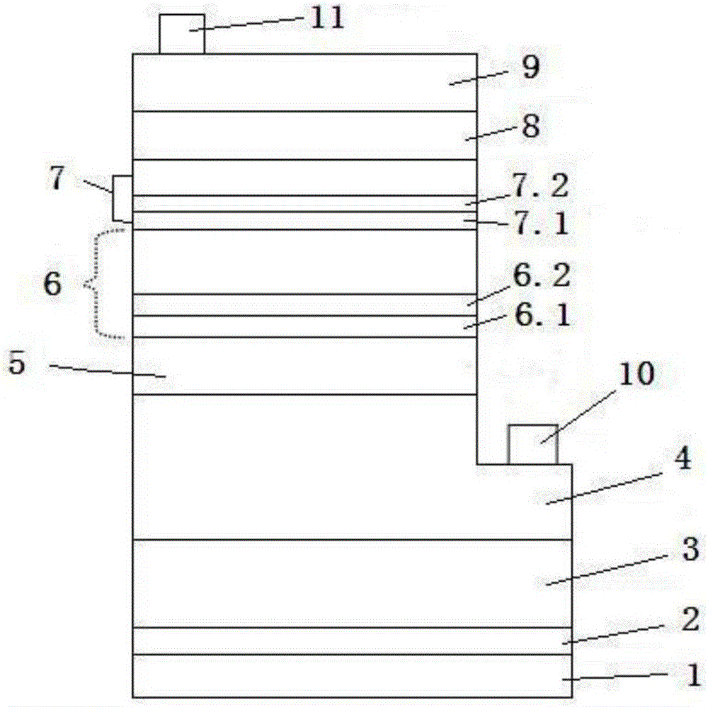
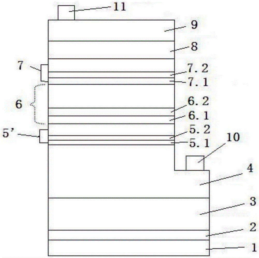
[0062] An LED epitaxial structure, see figure 2, including the following structure: from bottom to top, it includes sapphire substrate 1, low-temperature buffer layer 2, undoped GaN layer 3, Si-doped N-type GaN layer 4, light-emitting composite layer 5', light-emitting layer 6, superlattice layer 7, a first Mg-doped P-type ...
Embodiment 2
[0088] The only difference from Embodiment 1 is: the number of single pieces included in the optical composite layer 5', and the number of single pieces in this embodiment is 9.
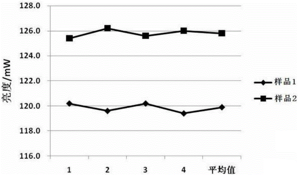
[0089] Sample 1 was prepared according to the existing LED growth method (see background art for details), and sample 2 and sample 3 were prepared according to the method of the present invention (Example 1-2). Samples 1-3 were plated with an ITO layer of about 150nm under the same pre-process conditions, plated with a Cr / Pt / Au electrode of about 70nm under the same conditions, and plated a protective layer of SiO under the same conditions 2 About 30nm, and then grind and cut the sample into (16mil*33mil) chip particles under the same conditions, and then test the photoelectric performance of samples 1-3 on the same testing machine, see brightness comparison for details image 3 , see the comparison of antistatic ability Figure 4 , because the effects of sample 3 and sample 2 are equivalent, so onl...
PUM
| Property | Measurement | Unit |
|---|---|---|
| thickness | aaaaa | aaaaa |
| thickness | aaaaa | aaaaa |
| thickness | aaaaa | aaaaa |
Abstract
Description
Claims
Application Information
 - Generate Ideas
- Intellectual Property
- Life Sciences
- Materials
- Tech Scout
- Unparalleled Data Quality
- Higher Quality Content
- 60% Fewer Hallucinations
Browse by: Latest US Patents, China's latest patents, Technical Efficacy Thesaurus, Application Domain, Technology Topic, Popular Technical Reports.
© 2025 PatSnap. All rights reserved.Legal|Privacy policy|Modern Slavery Act Transparency Statement|Sitemap|About US| Contact US: help@patsnap.com


