
A hermetic structure for wafer-level packaging and its manufacturing method

A wafer-level packaging and manufacturing method technology, which is applied in the process, microstructure technology, microstructure device and other directions for producing decorative surface effects, can solve the problems of complex process and high cost, and achieves mature technology, reduced volume, The effect of reducing packaging costs

Active Publication Date: 2018-02-02
RDA MICROELECTRONICS SHANGHAICO LTD
View PDF8 Cites 0 Cited by
  • Summary
  • Abstract
  • Description
  • Claims
  • Application Information

AI Technical Summary

Problems solved by technology

This document also uses metal packaging rings and two wafers together to form a sealed structure for wafer-level packaging. The process is relatively complicated and the cost is high, and through-silicon via technology is also required for wiring.

Method used


Image

  • A hermetic structure for wafer-level packaging and its manufacturing method
  • A hermetic structure for wafer-level packaging and its manufacturing method
  • A hermetic structure for wafer-level packaging and its manufacturing method

Examples


Embodiment Construction

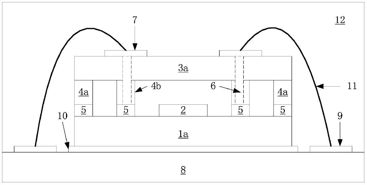
[0037] see figure 2 , which is Embodiment 1 of the airtight structure used for wafer-level packaging of semiconductor devices in this application. There are a plurality of semiconductor devices 2 on the base wafer 1, and the semiconductor devices 2 include MEMS devices and IC devices other than the MEMS devices. The periphery of each semiconductor device 2 is formed by a wall 13 to form an annular side wall, which in turn joins a roof 15 . The base chip unit 1a is obtained after the base wafer 1 is diced. The base chip unit 1a, the wall body 13 and the roof 15 constitute an airtight structure protecting each semiconductor device 2 . Wherein, the wall body 13 is made of photoresist material, and the roof 15 is made of photoresist or glass material, so it can be manufactured only by photolithography process and / or spin coating process. Preferably, the airtight structure is airtight, and the interior can be vacuum or filled with gas. The solder pads of each semiconductor dev...


PUM


Abstract

The invention discloses an airtight structure for wafer level encapsulation. Semiconductor devices are manufactured on a base wafer; an annular wall is formed at periphery of each semiconductor device on the base wafer with photoresist; roofs made of photoresist or glass materials are jointed at the upper sides of the walls; and the base wafer, the walls and the roofs form airtight structures so as to encapsulate each semiconductor device. Compared with the existing airtight structure for wafer level encapsulation, according to the structure disclosed by the invention, only one wafer is taken as one bottom surface; the photoresist is taken as the side walls; the photoresist or glass is taken as another bottom surface to form the airtight structures; the encapsulation size is clearly reduced; and the encapsulation cost can be reduced.

Description

technical field [0001] The present application relates to a wafer-level packaging technology for semiconductor devices. Background technique [0002] MEMS (Micro-Electro-Mechanical Systems) is an industrial technology that combines microelectronics and mechanical engineering. MEMS devices typically range in size from 20 microns to 1 mm, and are made up of components that typically range in size from 1 to 100 microns. MEMS usually includes a central unit that processes data (such as a microprocessor, microprocessor) and multiple components that interact with the external environment (such as a microsensor, microsensor). MEMS has the characteristics of miniaturization, intelligence, multi-function, and high integration. Common applications include accelerometers, gyroscopes, microphones, pressure sensors, filters, etc. [0003] MEMS manufacturing technology is developed on the basis of semiconductor manufacturing technology, including deposition, thermal oxidation, photolith...

Claims


Application Information

Patent Timeline
Patent Type & Authority Patents(China)
IPC IPC(8): B81B7/00B81C1/00H01L23/31H01L21/56
CPCH01L2224/48091
Inventor 祝明国胡念楚贾斌
Owner RDA MICROELECTRONICS SHANGHAICO LTD
Learn More