Nano dielectric layer preparation method based on thermal oxidation process
A technology of dielectric layer and thermal oxidation, which is applied in the direction of nanotechnology, nanotechnology, nanotechnology, etc. for materials and surface science, can solve problems such as unfavorable devices, interface defects, and complex operation of dielectric layers, so as to reduce defects and components uniform effect
- Summary
- Abstract
- Description
- Claims
- Application Information
AI Technical Summary
Problems solved by technology
Method used
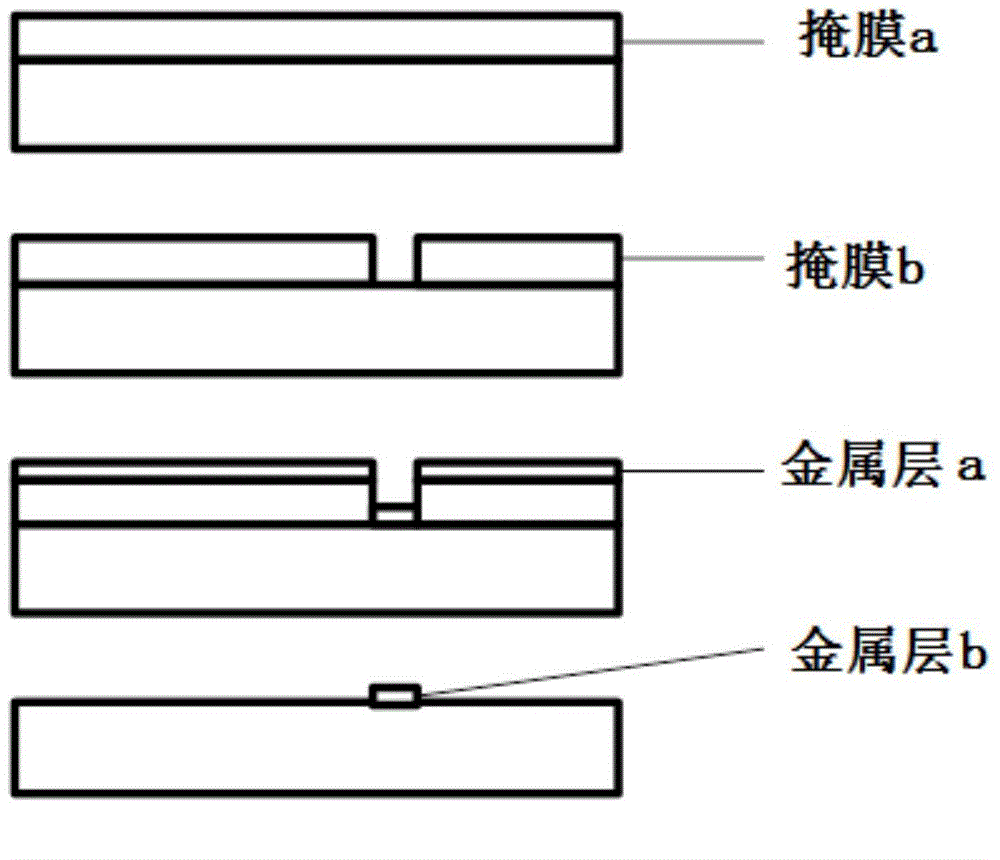
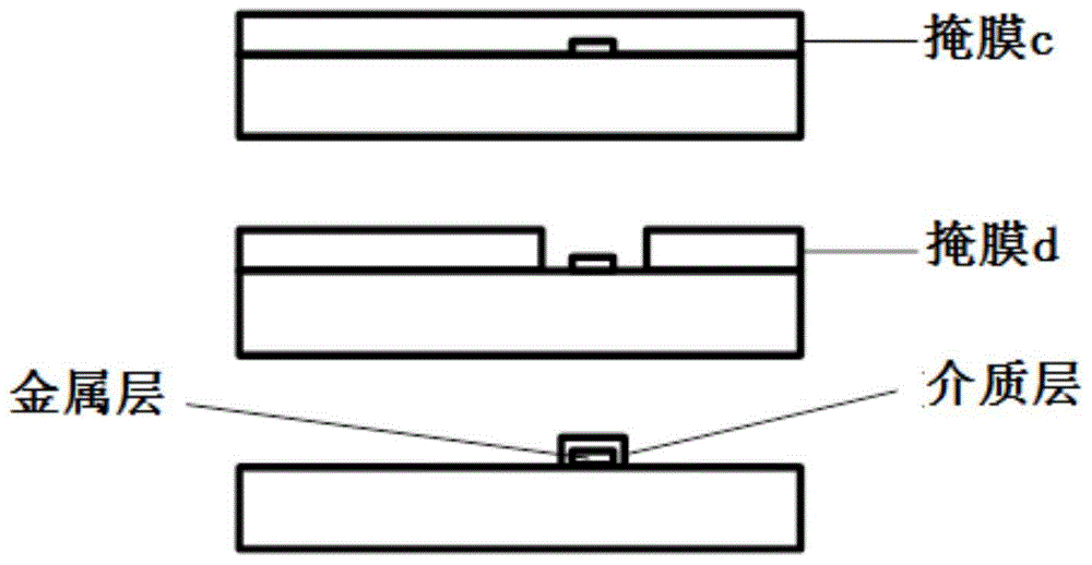
Image

Examples
Embodiment Construction
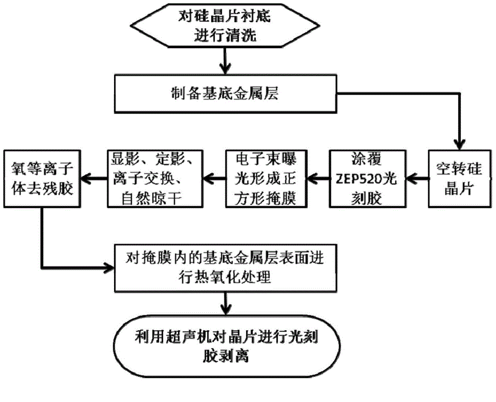
[0025] The present invention will be further described below in conjunction with accompanying drawing and example.
[0026] 1) Substrate cleaning
[0027] 11) The wafer used for the substrate is a silicon wafer with a 2 μm silicon dioxide layer. The specific cleaning steps are as follows: using an ultrasonic machine, soak the silicon wafer in acetone and sonicate at 40% power for 15 minutes, soak the silicon wafer in isopropanol and sonicate at 40% power for 15 minutes, wash it with deionized water, and dry it;
[0028] 12) Soak the silicon wafer in a mixture of concentrated sulfuric acid and hydrogen peroxide (5:1), heat it at 70°C for 15 minutes, and wash it with deionized water;
[0029] 13) Soak the silicon wafer in a mixture of water, hydrogen peroxide and ammonia (7:2:1), and heat at 70°C for 15 minutes;
[0030] 14) Soak the silicon wafer in a mixture of water, hydrogen peroxide and concentrated hydrochloric acid (7:2:1), heat at 70°C for 15min, wash with deionized wa...
PUM
 Abstract
Description
Claims
Application Information
 - R&D
- Intellectual Property
- Life Sciences
- Materials
- Tech Scout
- Unparalleled Data Quality
- Higher Quality Content
- 60% Fewer Hallucinations
Browse by: Latest US Patents, China's latest patents, Technical Efficacy Thesaurus, Application Domain, Technology Topic, Popular Technical Reports.
© 2025 PatSnap. All rights reserved.Legal|Privacy policy|Modern Slavery Act Transparency Statement|Sitemap|About US| Contact US: help@patsnap.com