Method for growing ultraviolet LED epitaxy structure

A technology of LED epitaxial wafers and epitaxial structures, which is applied in the direction of electrical components, circuits, semiconductor devices, etc., can solve the problems of low luminous efficiency and high voltage, and achieve the effects of easy heavy doping, lower contact voltage, and reduced absorption

Inactive Publication Date: 2014-07-09
西安利科光电科技有限公司
View PDF4 Cites 10 Cited by
  • Summary
  • Abstract
  • Description
  • Claims
  • Application Information

AI Technical Summary

Problems solved by technology

Ultraviolet LEDs can not only be used in the field of lighting, but also can replace traditional ultraviolet mercury lamps containing toxic and harmful substances in biomedicine, anti-counterfeiting identification, air and water purification, biochemical detection, and high-density information storage. Due to the limitations of the growth material itself and the difficulty of doping, the luminous efficiency is generally low, and the voltage is generally high. How to reduce the difficulty of doping and the difficulty of material growth is the focus of current research

Method used


Image

  • Method for growing ultraviolet LED epitaxy structure

Examples


Embodiment Construction

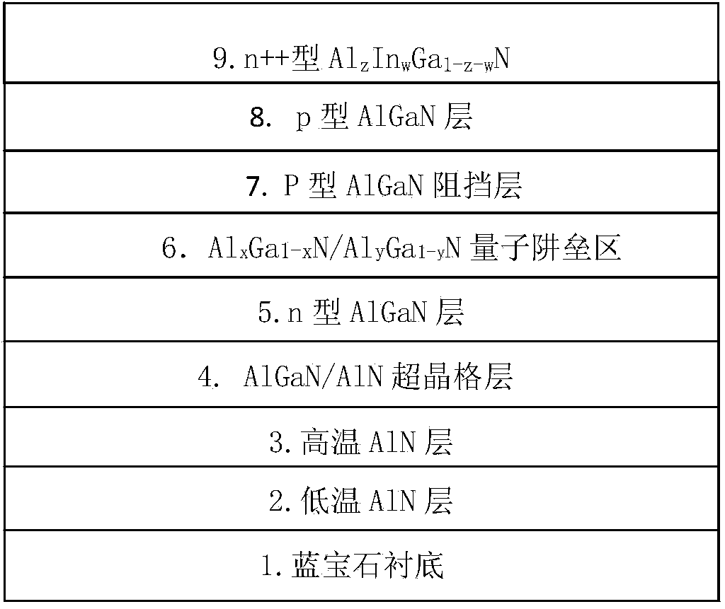
[0036] The invention adopts sapphire as a growth substrate to carry out heterogeneous epitaxial growth, and uses MOCVD (metal organic chemical vapor deposition) technology to complete the entire epitaxial process. Using trimethylgallium (TMGa), triethylgallium (TEGa), and trimethylindium (TMIn), trimethylaluminum (TMAl) and ammonia (NH3) silane (SiH4) and dimagnesocene (cp2mg) Provide gallium source, indium source, aluminum source, nitrogen source, silicon source and magnesium source required for growth respectively.

[0037] A layer of low-temperature AlN is grown on the sapphire substrate, and then a layer of AlN is grown at a high temperature, and then a few cycles of AlN / AlGaN superlattice structure layers are grown, and then a layer of n-type AlGaN doped with silane is grown, and then grown A layer of several periodic AlxGa1-xN / AlyGa1-yN (y>x) quantum well barrier regions, in which AlxGa1-xN is used as a well layer and AlyGa1-yN is used as a barrier layer. Then grow a ma...


PUM


Abstract

The invention discloses a method for growing an ultraviolet LED epitaxy structure. A new structural layer and a new surface contact layer are adopted for being doped, light can be prevented from being absorbed through surface materials when ultraviolet light is grown, and contact voltage can be further lowered. According to the method, a traditional magnesium-doped p-type GaN surface contact layer is replaced by the silane-doped n++-type AlzInwGa1-z-wN surface contact layer, the w is larger than 0 and smaller than 0.05, the z is larger than 0 and smaller than 0.9, absorption of GaN materials of the surface contact layer to the ultraviolet light is reduced, and the light emitting efficiency of an epitaxial wafer is improved; meanwhile, low-In-component n++-type AlzInwGa1-z-wN can be in good contact with an ITO current expanding layer of a chip manufacturing technology, heavy doping of n-type silane can be further easily achieved, good ohmic contact with the ITO layer can be formed, and the contact voltage can be reduced.

Description

technical field [0001] The invention belongs to the field of semiconductor optoelectronics and relates to a method for growing an epitaxial structure of a violet LED. Background technique [0002] With the development of LED applications, the market demand for ultraviolet LEDs is increasing. Ultraviolet LEDs with emission wavelengths covering 210-400nm have advantages that traditional ultraviolet light sources cannot match. Ultraviolet LEDs can not only be used in the field of lighting, but also can replace traditional ultraviolet mercury lamps containing toxic and harmful substances in biomedicine, anti-counterfeiting identification, air and water purification, biochemical detection, and high-density information storage. Due to the limitations of the growth material itself and the difficulty of doping, the luminous efficiency is generally low and the voltage is generally high. How to reduce the difficulty of doping and the difficulty of material growth is the focus of curre...

Claims


Application Information

Patent Timeline
Patent Type & Authority Applications(China)
IPC IPC(8): H01L33/00H01L33/30H01L33/06
CPCH01L33/007H01L33/06
Inventor 王晓波
Owner 西安利科光电科技有限公司
Why Eureka
Try Eureka