Light-emitting apparatus
a technology of light-emitting apparatus and diodes, which is applied in the direction of discharge tubes/lamp details, discharge tubes luminescnet screens, electric discharge lamps, etc., can solve the problems of low light-emitting efficiency of led devices, poor adhesion, reliability and peeling, etc., and achieve high light extraction efficiency and reduce the area of light extraction
- Summary
- Abstract
- Description
- Claims
- Application Information
AI Technical Summary
Benefits of technology
Problems solved by technology
Method used
Image
Examples
third embodiment
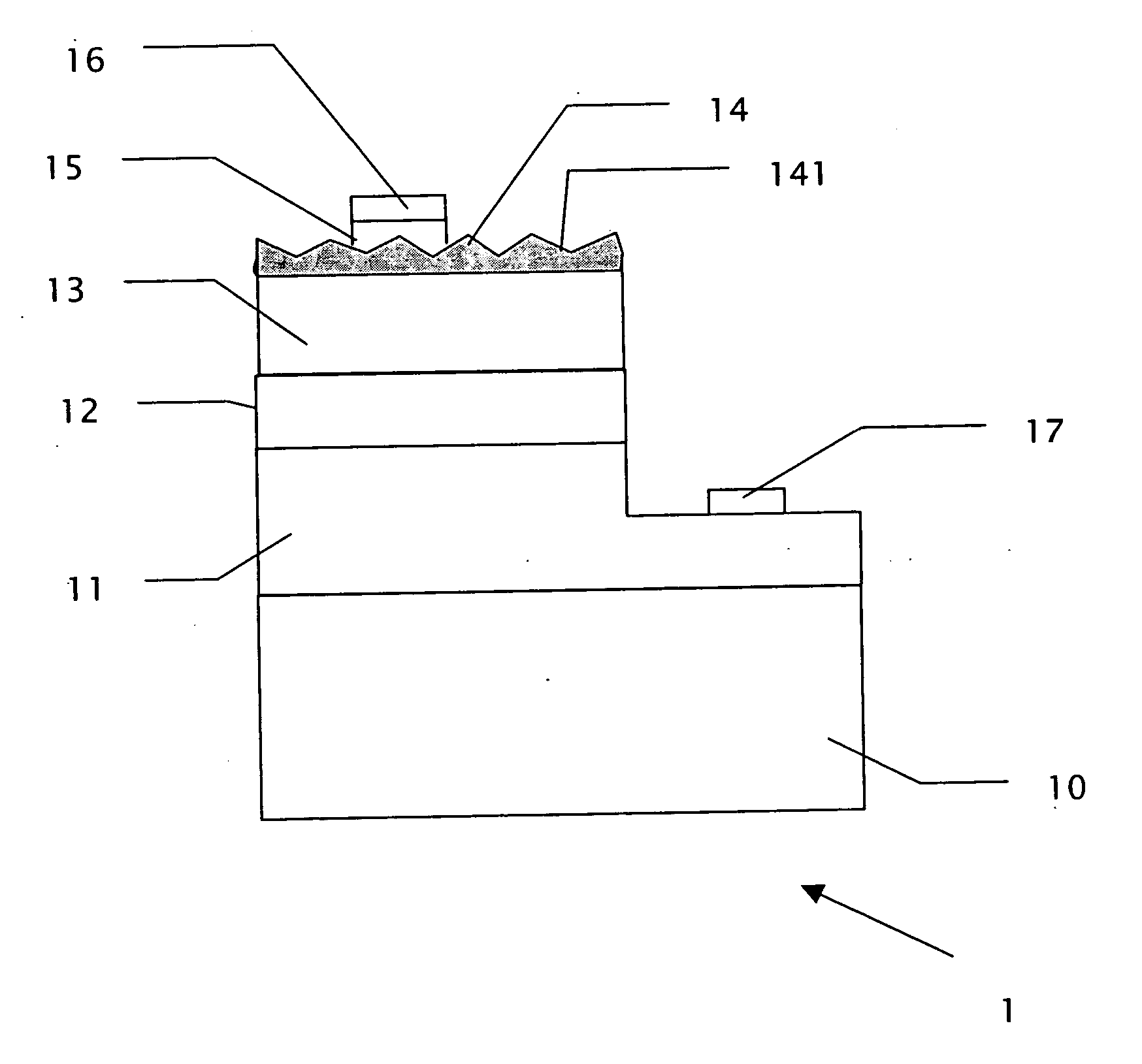
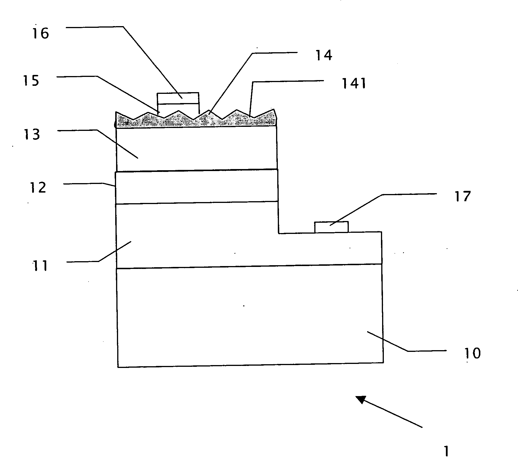
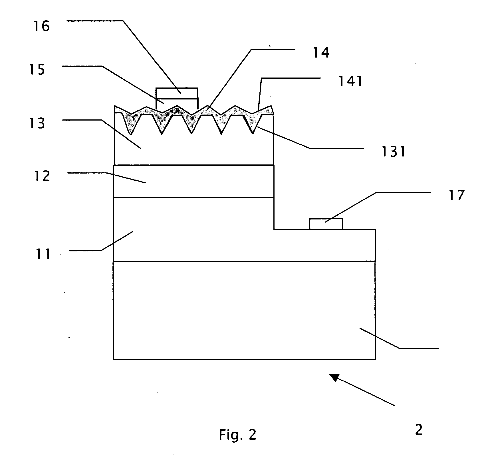
[0034] In addition, in accordance with the third embodiment, the second transparent conductive layer 18 can be formed directly on the first semiconductor layer 11 without the fourth plurality of cavities 111 and then an etching process is performed to form the third plurality of cavities 181.
[0035]FIG. 8 is a vertical sectional view of a light-emitting device 4 in accordance with a fourth embodiment of the present invention. The difference between the fourth embodiment and the first embodiment is that the substrate 10 is replaced by a conductive substrate 30, an additional Distributed Bragg Reflector layer (DBR layer) 31 is formed between the conductive substrate 30 and the first semiconductor layer 11, and a third electrode 37 is formed under the conductive substrate 30.
fifth embodiment
[0036]FIG. 9 is a vertical sectional view of a light-emitting device 5 in accordance with the present invention, which comprises a substrate 40, a reflective layer 41, a dielectric binding layer 42, a third transparent conductive oxide layer 43, a first semiconductor layer 44, a light-emitting layer 45, a second semiconductor layer 46, and a first transparent conductive oxide layer 47 stacked sequentially. The light-emitting device 5 further comprises a first plurality of cavities 471 on the upper surface of the first transparent conductive oxide layer 47, a first reflective metal layer 48 formed on the first plurality of cavities 471, a first electrode 491 formed on the first reflective metal layer 48 and a second electrode 492 formed on the third transparent conductive oxide layer 43.
sixth embodiment
[0037]FIG. 10 is a vertical sectional view of a light-emitting device 6 in accordance with the invention, which comprises a conductive substrate 50, a metal binding layer 51, a reflective layer 52, a third transparent conductive oxide layer 53, a first semiconductor layer 54, a light-emitting layer 55, a second semiconductor layer 56, and a first transparent conductive oxide layer 57 stacked sequentially. The light-emitting device 6 further comprises a first plurality of cavities 571 formed on the upper surface of the first transparent conductive oxide layer 57, a first reflective metal layer 58 formed on the first plurality of cavities 571, a first electrode 591 formed on the first reflective metal layer 58 and a second electrode 592 formed under the conductive substrate 50.
[0038] In the aforementioned embodiments, the substrates (10 and 40) are made of sapphire, SiC, GaAs, GaN, AlN, GaP, Si, ZnO, MgO, glass, or the combination thereof, and the conductive substrates (30 and 50) are...
PUM
| Property | Measurement | Unit |
|---|---|---|
| thickness | aaaaa | aaaaa |
| thickness | aaaaa | aaaaa |
| transparent | aaaaa | aaaaa |
Abstract
Description
Claims
Application Information
 - R&D
- Intellectual Property
- Life Sciences
- Materials
- Tech Scout
- Unparalleled Data Quality
- Higher Quality Content
- 60% Fewer Hallucinations
Browse by: Latest US Patents, China's latest patents, Technical Efficacy Thesaurus, Application Domain, Technology Topic, Popular Technical Reports.
© 2025 PatSnap. All rights reserved.Legal|Privacy policy|Modern Slavery Act Transparency Statement|Sitemap|About US| Contact US: help@patsnap.com


