Radio frequency transverse double-diffusion field effect transistor and manufacturing method thereof

A field-effect transistor and lateral double-diffusion technology, which is applied in semiconductor/solid-state device manufacturing, semiconductor devices, electrical components, etc., can solve problems such as increased electric field strength, HCI deterioration, and low on-resistance, so as to suppress injection and reduce Base resistance, effect of suppressing conduction

Inactive Publication Date: 2014-06-11
SHANGHAI HUAHONG GRACE SEMICON MFG CORP
View PDF14 Cites 8 Cited by
  • Summary
  • Abstract
  • Description
  • Claims
  • Application Information

AI Technical Summary

Problems solved by technology

In the application of RFLDMOS, sometimes a very large output power is required, so the device needs to have a very low on-resistance (Rdson). At this time, the concentration of the drift region will increase, and the original Faraday shielding layer remains unchanged. , the electric field intensity under the polysilicon gate oxide edge becomes larger, making HCI worse

Method used


Image

  • Radio frequency transverse double-diffusion field effect transistor and manufacturing method thereof
  • Radio frequency transverse double-diffusion field effect transistor and manufacturing method thereof
  • Radio frequency transverse double-diffusion field effect transistor and manufacturing method thereof

Examples


Embodiment Construction

[0063] In order to enable your examiners to have a further understanding and understanding of the purpose, features and effects of the present invention, the following detailed description is as follows with the accompanying drawings.

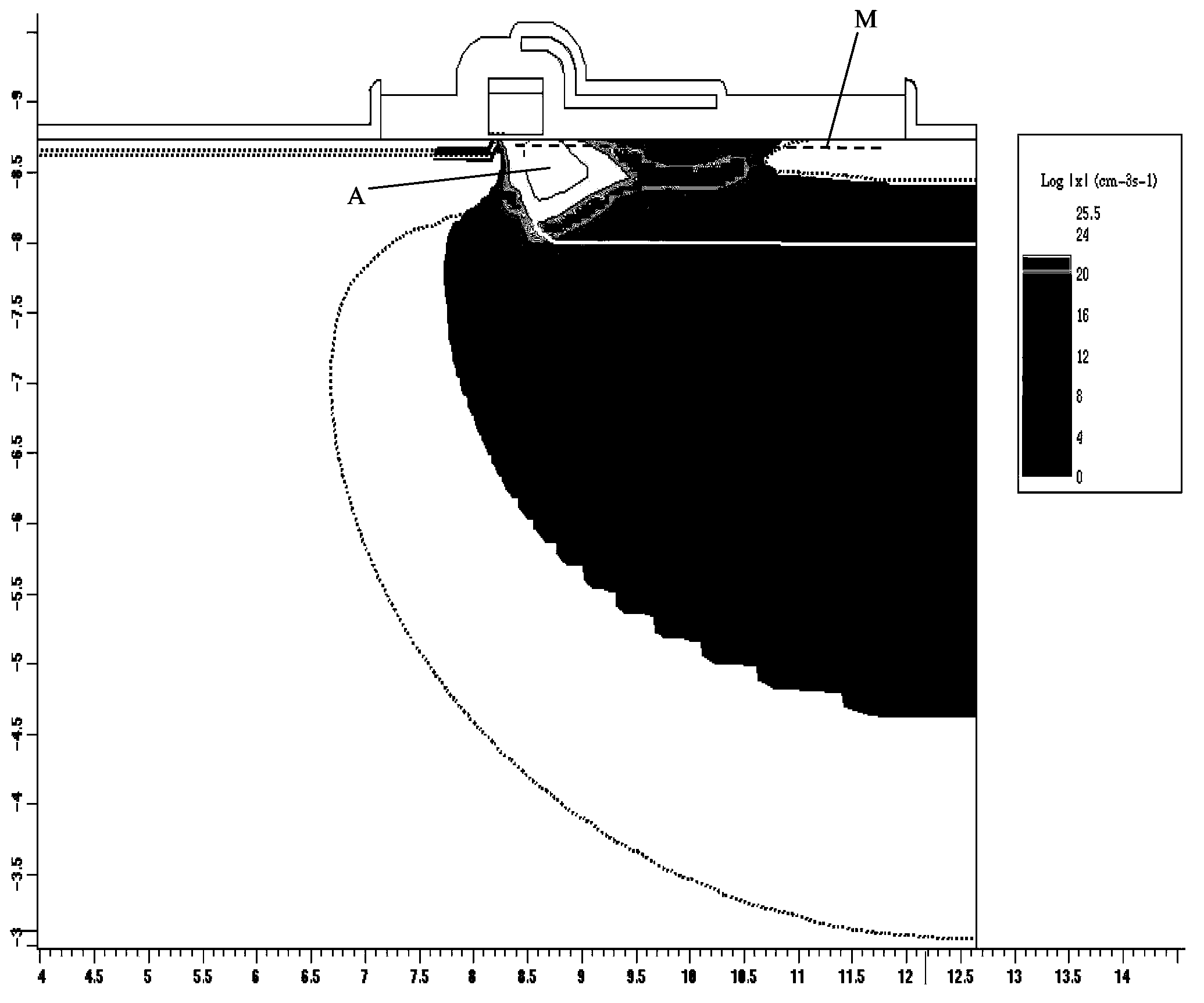
[0064] Such as figure 2 As shown, it is a schematic structural diagram of the first embodiment of the RFLDMOS device of the present invention. A substrate doped with a high-concentration P-type impurity, that is, a P-type substrate 201, is used on the P-type substrate 201 according to the requirements of the withstand voltage of the device. P-type epitaxial layers 202 with different thicknesses and doping concentrations are grown differently. In the P-type epitaxial layer 202, the region where the P buried layer 203 is etched is defined by a photolithography plate, that is, the source end to the region under the channel, and then P-type ion implantation and high temperature advance to form P buried layer 203; use ion implantation and diffusion...


PUM


Abstract

The invention discloses a radio frequency transverse double-diffusion field effect transistor. The radio frequency transverse double-diffusion field effect transistor comprises a P-type substrate, a P-type epitaxial layer and a P well, wherein the P-type epitaxial layer is formed on the P-type substrate in an epitaxial growth mode; the P well is located in the P-type epitaxial layer, formed in an ion injection mode and used for forming a channel; a P buried layer is arranged in the P-type epitaxial layer, formed in an ion injection mode and located below the P well, and makes contact with the P well. The radio frequency transverse double-diffusion field effect transistor can effectively lower base resistance of a parasitic bipolar transistor, thereby restraining the parasitic bipolar transistor from being conductive. The drift region with light dope runs out through the P buried layer and the P well together, electric fields on the surface of the drift region are evenly distributed, electric field intensity of the lower portion, close to the drain terminal edge, of a polysilicon gate is reduced, and therefore a hot carrier is restrained from being injected into an oxidation layer, close to the drain terminal edge, of the polysilicon gate.

Description

technical field [0001] The invention relates to a semiconductor integrated circuit, in particular to a radio frequency lateral double-diffusion field effect transistor, and also relates to a manufacturing method of the transistor. Background technique [0002] With the advent of the 3G era, more and more communication fields require the development of more powerful radio frequency (RF) devices. Radio Frequency Lateral Double Diffused Field Effect Transistor (RFLDMOS), due to its very high output power, has been widely used in portable wireless base station power amplification as early as the 1990s, and its application frequency is 900MHz-3.8GHz. Compared with traditional silicon-based bipolar transistors, RFLDMOS has better linearity, higher power and gain. Today, RFLDMOS is more popular than bipolar, and GaAs devices. [0003] In the reliability evaluation of RFLDMOS, hot carrier injection (HCI) and whether the parasitic bipolar transistor is easy to turn on are two very ...

Claims


Application Information

Patent Timeline
Patent Type & Authority Applications(China)
IPC IPC(8): H01L29/78H01L29/06H01L21/336
CPCH01L29/7835H01L29/1041H01L29/1083H01L29/402H01L29/4175H01L29/7816H01L29/0684H01L29/66681
Inventor 李娟娟钱文生韩峰慈朋亮
Owner SHANGHAI HUAHONG GRACE SEMICON MFG CORP
Why Eureka
Try Eureka