Standard comprehensive target board for rapid self-calibration of photoelectric system and measurement method for photoelectric system
A photoelectric system, a standard technology, applied in the direction of measuring devices, target indicating systems, optical instrument testing, etc., can solve the problems of measurement speed limitation, insufficient brightness, etc.
- Summary
- Abstract
- Description
- Claims
- Application Information
AI Technical Summary
Problems solved by technology
Method used
Image
Examples
Embodiment 1
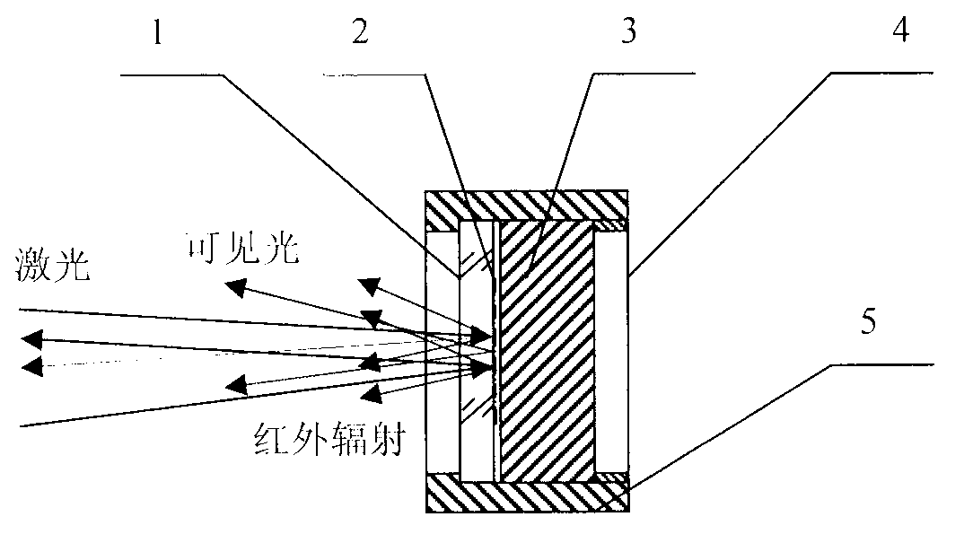
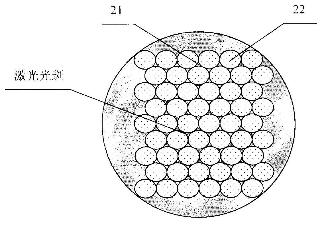
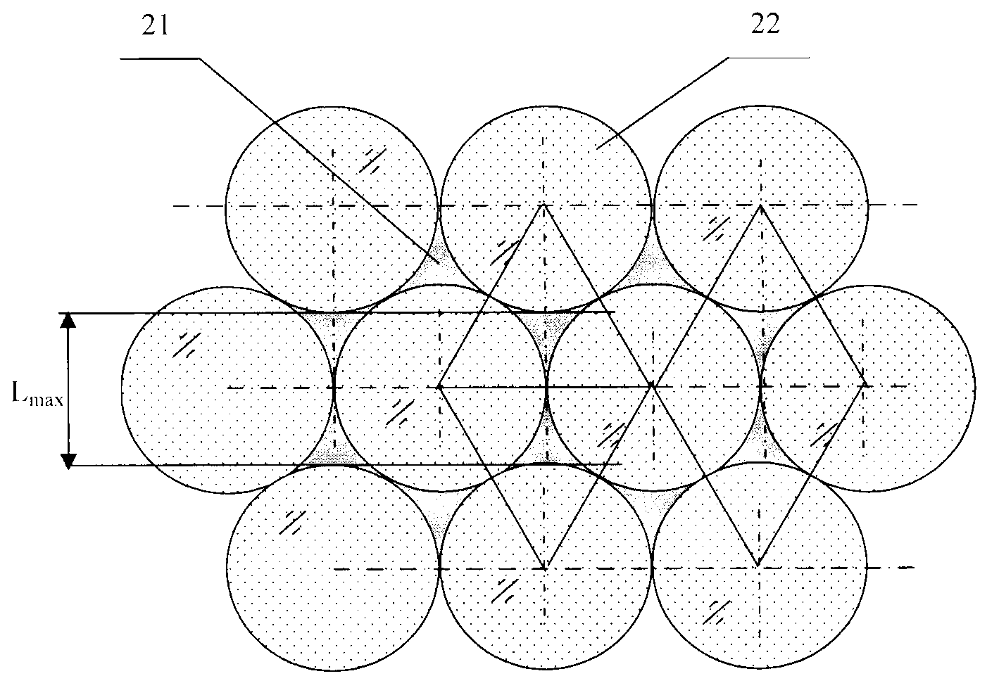
[0043] according to figure 1 As shown, the preferred embodiment of the present invention provides a standard integrated target plate used on the focal plane of a collimator with a focal length of 3 m, including a substrate 1, a pattern 2, a base 3, and a pressure ring 4, which are sequentially tightly packed in a housing 5, it is characterized in that: the substrate 1 is an optical flat plate that transmits laser light, visible light, and infrared radiation. In this embodiment, a silicon carbide crystal flat plate is preferred, with a diameter of 8 mm and a thickness of 300 μm. The pattern 2 is attached to the substrate 1. Multi-layer metal film 21, nano display powder 22 composition; In this embodiment, it is preferred to plate tungsten thin film and then gold thin film on substrate 1, according to figure 2 , image 3 As shown, a through-hole array with a diameter of 10 μm and a hole spacing of 12 μm is etched on the metal film 21 by photolithography. The through holes are...
Embodiment 2
[0061] according to figure 1 As shown, the preferred embodiment 2 of the present invention provides a standard comprehensive target plate for placing at a distance of 100m, including a substrate 1, a pattern 2, a base 3, and a pressure ring 4, which are tightly packed in a housing 5 in turn, and its characteristics In that: the substrate 1 is an optical flat plate that transmits laser light, visible light, and infrared radiation. In this embodiment, the preferred sapphire flat glass has a diameter of 150 mm and a thickness of 3 mm. The pattern 2 consists of a metal film layer 21 attached to the substrate 1, Micro-nano display powder 22 composition; the preferred gold-plated film material in this embodiment, according to figure 2 , image 3 As shown, an electroplating process is adopted on the metal film 21 and an array of through holes with a diameter of 6 mm and a hole spacing of 7 mm is etched. The centers of adjacent through holes form an equilateral triangle. The throug...
PUM
 Abstract
Description
Claims
Application Information
 - R&D
- Intellectual Property
- Life Sciences
- Materials
- Tech Scout
- Unparalleled Data Quality
- Higher Quality Content
- 60% Fewer Hallucinations
Browse by: Latest US Patents, China's latest patents, Technical Efficacy Thesaurus, Application Domain, Technology Topic, Popular Technical Reports.
© 2025 PatSnap. All rights reserved.Legal|Privacy policy|Modern Slavery Act Transparency Statement|Sitemap|About US| Contact US: help@patsnap.com


