Silicon on insulator (SOI)-based metal-oxide-semiconductor field-effect transistor (PMOSFET) power device
A power device, N-type technology, applied in the direction of semiconductor devices, electrical components, circuits, etc., can solve the problem that the breakdown voltage of the device is very sensitive and is larger than the on-resistance, etc., to improve the breakdown voltage and drift region concentration. , the effect of reducing the on-resistance and reducing the lateral size
- Summary
- Abstract
- Description
- Claims
- Application Information
AI Technical Summary
Problems solved by technology
Method used
Image

Examples
Embodiment 1
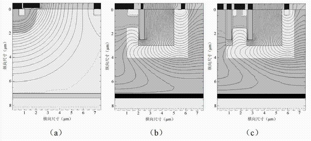
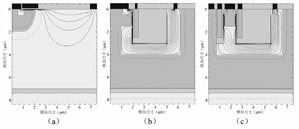
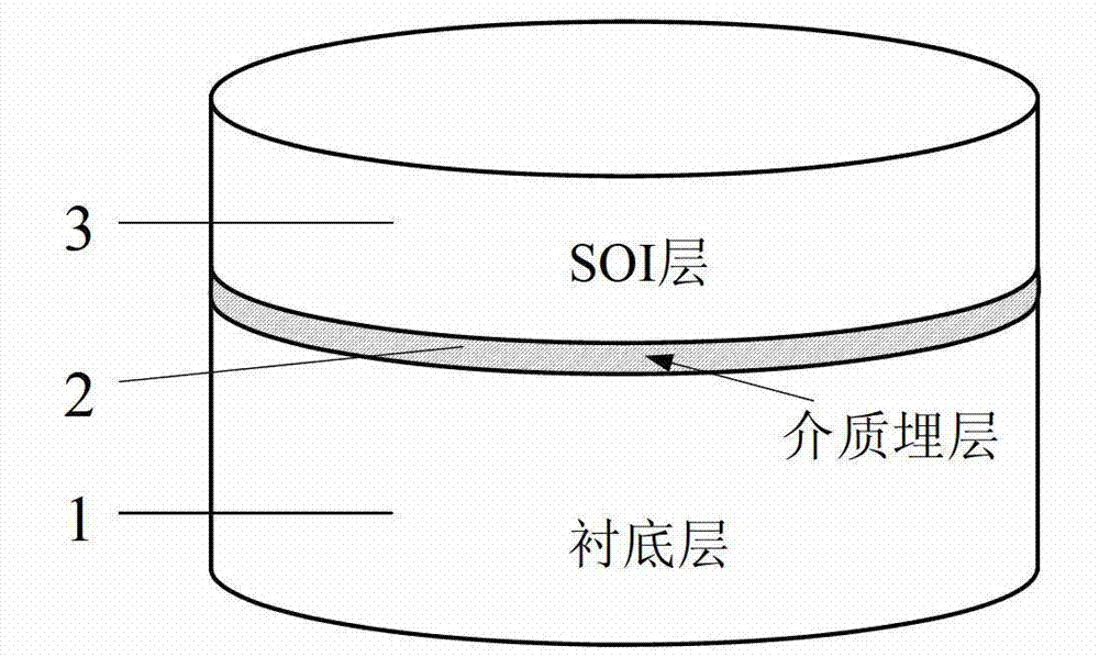
[0040] A SOI-based PMOSFET power device, such as Figure 5 As shown, it includes an N-type SOI base formed by vertically bottom-up substrate layer 1, dielectric buried layer 2 and N-type SOI semiconductor layer 3; the N-type SOI semiconductor layer 3 is lightly doped N-type A semiconductor layer (N-type high-resistance region), which has a P-type well region 4; the other surfaces of the P-type well region 4 except the upper surface are all in contact with the N-type SOI semiconductor layer 3; the P-type well region has The dielectric groove 6 is filled with an insulating medium 9; the dielectric groove 6 is horizontally ( Figure 5 The surface of the P-type well region 4 on one side of the shown x direction) has a P-type heavily doped (P+) drain region 14, and the surface of the P-type heavily doped drain region 14 leads to the drain electrode (D) through the drain metal; the dielectric The top of the P-type well region 4 on the other lateral side of the groove 6 has an N-typ...
Embodiment 2
[0042] Such as Figure 6 As shown, on the basis of Embodiment 1, the N-type body region 5 extends into the top of the N-type SOI semiconductor layer 3, and the N-type heavily doped low-resistance region 13 merges into the N-type heavily doped body contact region 12 form the same N-type heavily doped body contact region 12 .
Embodiment 3
[0044] Such as Figure 7 As shown, on the basis of Example 1, the N-type body region 5 also has a second P-type heavily doped source region 11b, and the N-type heavily doped body contact region 12 is sandwiched between the P-type heavily doped source Between the region 11 and the second P-type heavily doped source region 11b, the lead end of the second P-type heavily doped source region 11b is electrically connected to the source electrode; the second P-type heavily doped source region 11b and the The surfaces of the P-type well region 4 and the N-type body region 5 between the N-type heavily doped low-resistance regions 13 have a planar gate structure 8, and the leading end of the planar gate structure 8 is electrically connected to the gate electrode. In this way, there is a certain distance between the N-type body region 5 and the N-type high-resistance region 13 in the lateral direction, so as to provide a conduction current channel. Compared with the structures of Exampl...
PUM
 Abstract
Description
Claims
Application Information
 - R&D
- Intellectual Property
- Life Sciences
- Materials
- Tech Scout
- Unparalleled Data Quality
- Higher Quality Content
- 60% Fewer Hallucinations
Browse by: Latest US Patents, China's latest patents, Technical Efficacy Thesaurus, Application Domain, Technology Topic, Popular Technical Reports.
© 2025 PatSnap. All rights reserved.Legal|Privacy policy|Modern Slavery Act Transparency Statement|Sitemap|About US| Contact US: help@patsnap.com