Monolayer organic solar cell and preparation method thereof
A solar cell and organic technology, applied in circuits, electrical components, photovoltaic power generation, etc., can solve the problems of demanding heterojunction growth control, increasing the complexity of organic solar cell devices, etc., to improve energy conversion efficiency and reduce production costs. , the effect of stable performance
- Summary
- Abstract
- Description
- Claims
- Application Information
AI Technical Summary
Problems solved by technology
Method used
Image
Examples
preparation example Construction
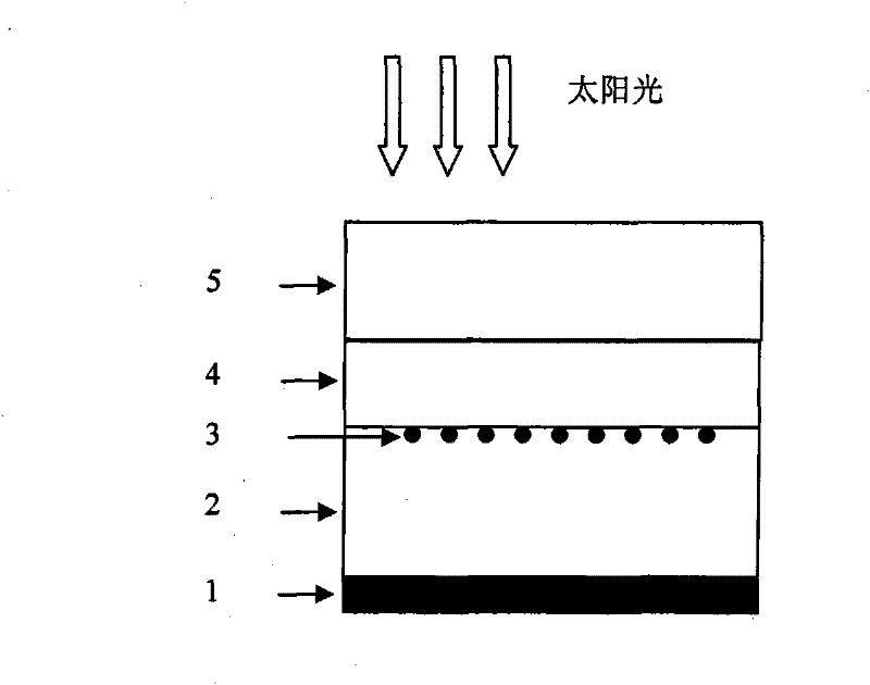
[0028] This embodiment also provides a method for preparing a single-layer organic solar cell device, comprising the following steps:
[0029] 1) Obtain a transparent insulating substrate 5;
[0030] 2) forming a transparent anode electrode layer 4 on one side of the transparent insulating substrate 5;
[0031] 3) forming a metal nanoparticle layer 3 on the transparent anode electrode layer 4, the work function value of the metal nanoparticles in the metal nanoparticle layer 3 is higher than the work function value of the transparent anode electrode layer 4;
[0032] 4) Depositing a photosensitive material on the metal nanoparticle layer 3 to form a photosensitive layer 2;
[0033] 5) Depositing a metal or metal oxide thin film on the photosensitive layer 2 to form the cathode electrode layer 1, thereby obtaining the single-layer organic solar cell.
[0034] In above-mentioned step 1), the thickness of transparent insulating substrate 5 is preferably 1.1-1.5mm, and its mater...
Embodiment 1
[0041] The structure of a single-layer organic solar cell is as figure 1 As shown, the high-reflectivity cathode electrode layer 1 adopts an aluminum film electrode, the photosensitive layer 2 adopts a CuPc copper phthalocyanine thin film, the metal nanoparticle layer 3 is a gold nanoparticle, and the transparent transparent anode electrode layer 4 adopts an ITO stripe electrode, and its square resistance is 15 ohm / □, the transparent insulating substrate 5 is made of quartz glass.
[0042] Its specific preparation method is as follows:
[0043] (1) Select polished quartz glass with a thickness of 1.1mm as the transparent insulating substrate 5, and use an ultrasonic method to clean the quartz glass for 2-3 hours;
[0044] (2) adopt the method for sputtering to grow one deck ITO conductive thin film on one surface of quartz glass, and the thickness of ITO thin film is 120nm;
[0045] (3) Photoetching the ITO conductive film into the required striped electrode pattern as the t...
Embodiment 2
[0051] like figure 1 As shown, the high-reflectivity cathode electrode layer 1 adopts a silver thin film electrode, the photosensitive layer 2 adopts a pentacene thin film, the metal nanoparticle layer 3 is a gold nanoparticle, and the transparent anode electrode layer 4 adopts an ITO stripe electrode, and its square resistance is 15 ohms / □, the transparent insulating substrate 5 is made of quartz glass.
[0052] Its specific preparation method is as follows:
[0053] (1) Select polished quartz glass with a thickness of 1.5mm as the transparent insulating substrate 5, and use an ultrasonic method to clean the quartz glass for 2-2.5 hours;
[0054] (2) adopt the method for sputtering to grow one deck ITO conductive thin film on one surface of quartz glass, and the thickness of ITO thin film is 80nm;
[0055] (3) Photoetching the ITO conductive film into the required stripe electrode pattern as the anode of the solar cell; as the transparent anode electrode layer 4, that is, ...
PUM
| Property | Measurement | Unit |
|---|---|---|
| thickness | aaaaa | aaaaa |
| thickness | aaaaa | aaaaa |
| thickness | aaaaa | aaaaa |
Abstract
Description
Claims
Application Information
 - R&D
- Intellectual Property
- Life Sciences
- Materials
- Tech Scout
- Unparalleled Data Quality
- Higher Quality Content
- 60% Fewer Hallucinations
Browse by: Latest US Patents, China's latest patents, Technical Efficacy Thesaurus, Application Domain, Technology Topic, Popular Technical Reports.
© 2025 PatSnap. All rights reserved.Legal|Privacy policy|Modern Slavery Act Transparency Statement|Sitemap|About US| Contact US: help@patsnap.com


