N type doped silicon film, preparation method of N type doped silicon film and solar cell comprising N type doped silicon film
A solar cell and silicon-doped technology, which is applied in the field of solar cells, can solve problems such as the reduction of conversion efficiency of solar cells, and achieve the effects of reducing energy consumption, improving conversion efficiency, and reducing series resistance
- Summary
- Abstract
- Description
- Claims
- Application Information
AI Technical Summary
Problems solved by technology
Method used
Image

Examples
preparation example Construction
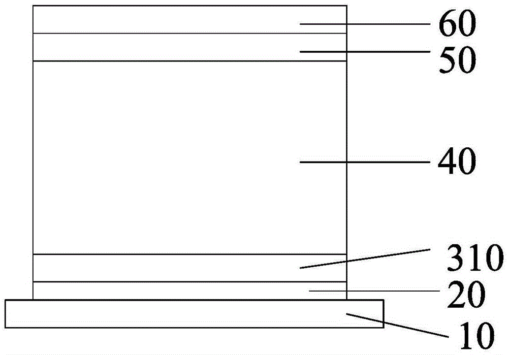
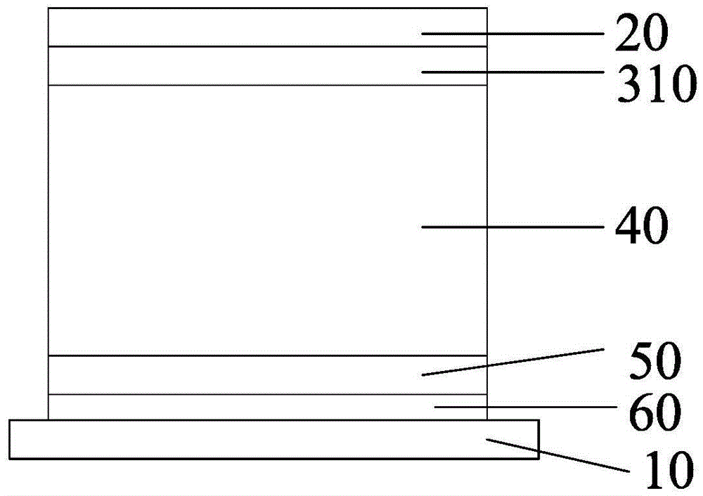
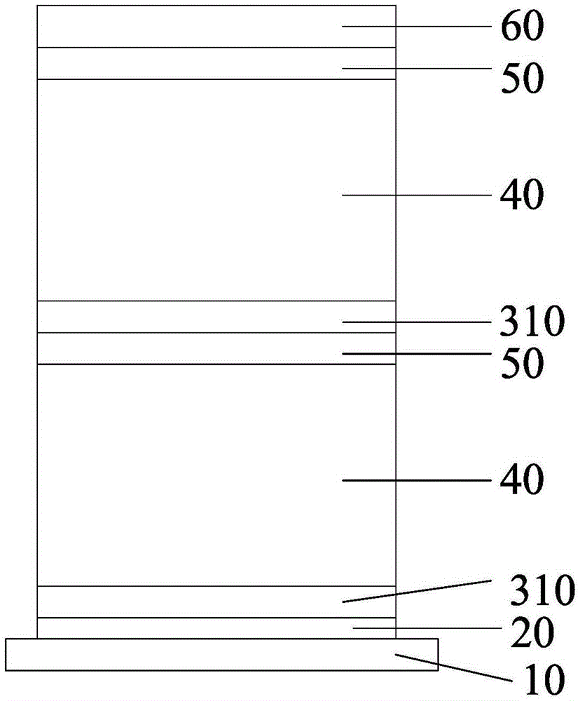
[0030] It can be seen from the background art that the N-type doped silicon thin film prepared from the amorphous silicon thin film in the prior art reduces the conversion efficiency of the solar cell. The inventors of the present invention have conducted research on the above problems and provided a method for preparing an N-type doped silicon film, which includes the following steps: depositing an N-type doped silicon film on a semi-finished solar cell located in a reaction chamber using a plasma-enhanced chemical vapor deposition process. Doped silicon film, the reaction gas of the plasma enhanced chemical vapor deposition process includes silicon source gas, hydrogen gas and dopant gas, wherein, the flow ratio of hydrogen gas to silicon source gas is 80:1~150:1, and the plasma enhanced chemical vapor deposition process is carried out. During the deposition process, the surface temperature of the semi-finished solar cell is 50-70°C, and the glow power density of the plasma-e...
Embodiment 1
[0048] The preparation method of the N-type doped silicon thin film of the present embodiment comprises the following steps:
[0049] Vacuumize the reaction chamber so that the degree of vacuum in the reaction chamber is 10 -5 Pa;
[0050] The PECVD process is used to deposit and form N-type doped silicon films on the semi-finished solar cells located in the reaction chamber. The reactive gas of the plasma-enhanced chemical vapor deposition process includes silicon source gas SiH 4 , hydrogen and dopant gas PH 3 , wherein the flow ratio of hydrogen to silicon source gas is 80:1, the flow ratio of dopant gas to silicon source gas is 1:5, when PECVD process is carried out, the surface temperature of semi-finished solar cell is 50°C, plasma enhanced chemical vapor phase The glow power density of the deposition process is 0.8W / cm 2 , the reaction pressure is 500Pa, and the power frequency is 13.56MHz.
Embodiment 2
[0052] The preparation method of the N-type doped silicon thin film of the present embodiment comprises the following steps:
[0053] Vacuumize the reaction chamber so that the degree of vacuum in the reaction chamber is 10 -5 Pa;
[0054] The PECVD process is used to deposit and form N-type doped silicon films on the semi-finished solar cells located in the reaction chamber. The reactive gas of the plasma-enhanced chemical vapor deposition process includes the silicon source gas Si 2 h 6 , hydrogen and dopant gas AsH 3 , wherein the flow ratio of hydrogen to silicon source gas is 150:1, the flow ratio of dopant gas to silicon source gas is 1:10, when PECVD process is carried out, the surface temperature of semi-finished solar cell is 70°C, plasma enhanced chemical vapor phase The deposition process has a glow power density of 1.5W / cm 2 , the reaction pressure is 750Pa, and the power frequency is 13.56MHz.
PUM
| Property | Measurement | Unit |
|---|---|---|
| particle size | aaaaa | aaaaa |
| particle size | aaaaa | aaaaa |
Abstract
Description
Claims
Application Information
 - R&D
- Intellectual Property
- Life Sciences
- Materials
- Tech Scout
- Unparalleled Data Quality
- Higher Quality Content
- 60% Fewer Hallucinations
Browse by: Latest US Patents, China's latest patents, Technical Efficacy Thesaurus, Application Domain, Technology Topic, Popular Technical Reports.
© 2025 PatSnap. All rights reserved.Legal|Privacy policy|Modern Slavery Act Transparency Statement|Sitemap|About US| Contact US: help@patsnap.com