Plasma separating chip and preparation method thereof
A plasma separation and chip technology, applied in the field of microelectromechanical systems, can solve the problems of high consumption of sample biochemical reagents, restricting the development of biochemical analysis, and difficulty in realizing automation, and achieves the effects of compact structure, reduced total area, and short time consumption.
- Summary
- Abstract
- Description
- Claims
- Application Information
AI Technical Summary
Problems solved by technology
Method used
Image

Examples
Embodiment 1
[0060] Embodiment 1: Process a chip on a silicon wafer
[0061] The structure of this embodiment refers to the attached figure 1 , see the appendix for the process flow figure 2 .
[0062] 1) Silicon wafer structure process:
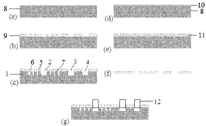
[0063] (a) processing and cleaning the silicon wafer 8;
[0064] (b) Throwing the photoresist 9 on the front side of the silicon wafer, pre-baking, photolithography, developing, and post-baking;
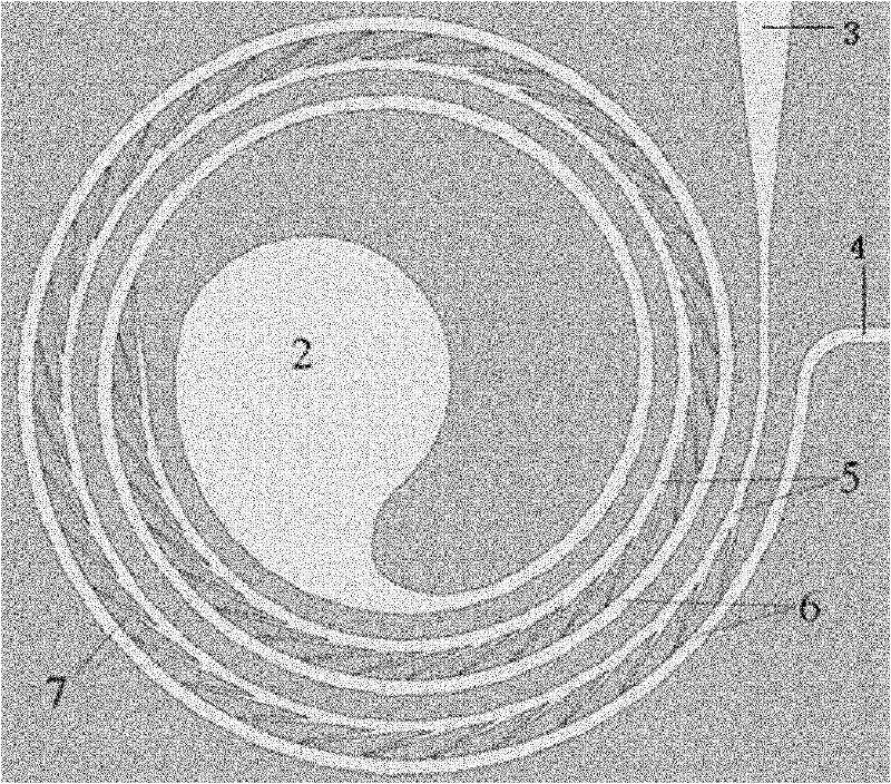
[0065] (c) In-depth etching (ICP) of about 100 μm of silicon on the front side of the silicon wafer to form a microfluidic channel 4, a microcolumn array separator 1, a sample inlet 2, and two sample outlets 3 and 4;
[0066] 2) Cover slip polymer process:
[0067] (d) process and clean the silicon wafer 8, and apply a release agent 10 on its surface;
[0068] (e) Pour the bubble-free silicon rubber photoresist (PDMS) 11 into the petri dish, let it stand for flattening, and then bake it in an oven at 80°C for about 1 hour;
[0069] (f) The cured PDMS11 ...
Embodiment 2
[0071] Example 2: Process chips with polymers
[0072] The structure of this embodiment refers to the attached figure 1 , see the appendix for the process flow image 3 .
[0073] 1) Process flow of polymer structure:
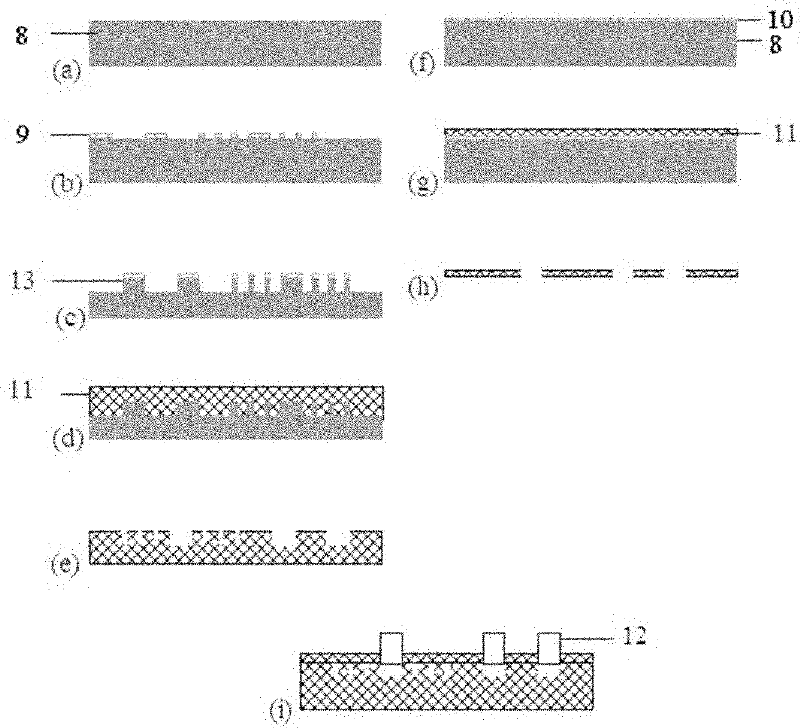
[0074] (a) processing and cleaning the silicon wafer 8;
[0075] (b) Throwing the photoresist 9 on the front side of the silicon wafer, pre-baking, photolithography, developing, and post-baking;
[0076] (c) In-depth etching (ICP) of about 100 μm of silicon on the front side of the silicon wafer to form microfluidic channels 4, gradient channels, sample inlets and sample outlets;
[0077] (d) Process and clean the silicon structure mold 13, and apply a release agent 10 on its surface, pour the bubble-free PDMS 11 on the silicon structure mold 13, and let it stand for flattening, then bake in an oven at 80°C Bake for about 1 hour;
[0078] (e) peel off the cured PDMS from the silicon mold 13, and cut each unit;
[0079] 2) Cover slip polymer process:
[...
Embodiment 3
[0084] Example 3: Sandwich structure
[0085] The structure of this embodiment refers to the attached figure 1 , see the appendix for the process flow Figure 4 .
[0086] (a) processing and cleaning the silicon wafer 8;
[0087] (b) Throwing the photoresist 9 on the front side of the silicon wafer, pre-baking, photolithography, developing, and post-baking;
[0088] (c) In-depth etching (ICP) silicon about 50 μm on the front side of the silicon wafer to form microfluidic channels 5, 6 and gradient channels (similar to method 1 structure);
[0089] (d) the front side of the silicon wafer is anodically bonded to the glass 14;
[0090] (e) Thinning the silicon wafer on the back side of the silicon glass sheet after bonding, the method of dry method, wet method or CMP can be adopted;
[0091] (f) Photoresist removal on the back of the silicon wafer, pre-baking, photolithography, development, and post-baking;
[0092] (g) Deeply etch the inlet and outlet sample ports;
[009...
PUM
| Property | Measurement | Unit |
|---|---|---|
| width | aaaaa | aaaaa |
| width | aaaaa | aaaaa |
| diameter | aaaaa | aaaaa |
Abstract
Description
Claims
Application Information
 - R&D
- Intellectual Property
- Life Sciences
- Materials
- Tech Scout
- Unparalleled Data Quality
- Higher Quality Content
- 60% Fewer Hallucinations
Browse by: Latest US Patents, China's latest patents, Technical Efficacy Thesaurus, Application Domain, Technology Topic, Popular Technical Reports.
© 2025 PatSnap. All rights reserved.Legal|Privacy policy|Modern Slavery Act Transparency Statement|Sitemap|About US| Contact US: help@patsnap.com