Epitaxial thin film used for high-dielectric constant gate dielectric and preparation method thereof

A technology of high dielectric constant and epitaxial thin film, which is applied in the manufacture of circuits, electrical components, semiconductor/solid-state devices, etc. It can solve the problems of low crystallization, application limitations, large leakage current, etc., and achieve high dielectric constant and conduction band Effect of offset, stable thermodynamic properties, high crystallization temperature

Inactive Publication Date: 2010-06-23
GENERAL RESEARCH INSTITUTE FOR NONFERROUS METALS BEIJNG
View PDF0 Cites 8 Cited by
  • Summary
  • Abstract
  • Description
  • Claims
  • Application Information

AI Technical Summary

Problems solved by technology

[0005] 1. The oxide and Si substrate will inevitably form an intermediate transition layer at the interface due to the problem of oxygen diffusion, which usually greatly reduces the effective dielectric constant of the gate dielectric layer
Rare earth metals are also easy to form silicides with Si, making high-k oxides unable to be used as gate dielectric layers in field effect transistors
[0006] 2. Although rare earth oxides generally have higher dielectric constants and conduction band offsets than hafnium oxides, their applications are limited due to their low crystallization problems
[0007] 3. Epitaxial thin films have attracted attention due to their smaller bulk defects, however, usually HfO 2 The lattice mismatch between the material and the semiconductor substrate is large, and the obtained epitaxial film has dislocations such as grain boundaries and kinks, resulting in excessive leakage current

Method used


Image

  • Epitaxial thin film used for high-dielectric constant gate dielectric and preparation method thereof
  • Epitaxial thin film used for high-dielectric constant gate dielectric and preparation method thereof
  • Epitaxial thin film used for high-dielectric constant gate dielectric and preparation method thereof

Examples


Embodiment Construction

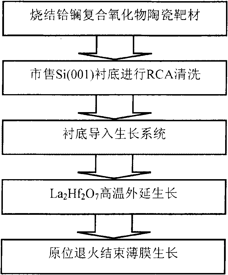
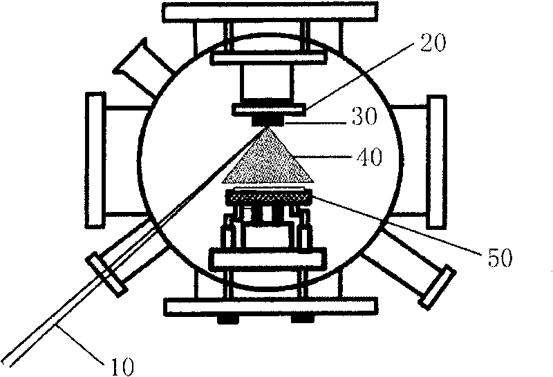
[0034] like figure 1 As shown in the technological process of the present invention, the preparation method of preparing high-k gate dielectric thin film material on Si(001) substrate is as follows:

[0035] 1. Sintered hafnium-lanthanum composite oxide ceramic target: first obtain a pyrochlore phase (A 2 B 2 o 7 ) hafnium-lanthanum composite oxide ceramic target. HfO with a purity of 99.9995% is first proportionally 2 with a purity of 99.9995% La 2 o 3 Mixing is carried out under the condition of high-purity ball milling (95-type zirconia balls), and then the powder is calcined at 600°C to obtain an average particle size of 500-800nm. Then the powder is pressed into a disc with a diameter of 40mm and a thickness of 4mm by uniaxial cold pressing and cold isostatic pressing, and is fully reacted and sintered at 1450-1550°C in an oxygen-containing atmosphere to form a dense ceramic target.

[0036] 2. RCA cleaning of commercially available Si(001) substrates: Surface trea...


PUM

PropertyMeasurementUnit
thicknessaaaaaaaaaa
wavelengthaaaaaaaaaa
diameteraaaaaaaaaa

Abstract

The invention relates to a material used for a high-dielectric constant (high-k) gate dielectric in a new generation integrated circuit field-effect tube and a preparation method thereof. The epitaxial thin film material used for the high-dielectric constant gate dielectric is a single high-oriented epitaxial thin film on an Si(001) underlay; the thin film is a single-crystalline state hafnium-lanthanum composite oxide La2Hf2O7 with a pyrochlore phase structure; and the crystallographic orientation relationship between the thin film and the Si(001) underlay is La2Hf2O7(001)//Si(001). In the preparation method of the epitaxial thin film, a hafnium-lanthanum composite oxide (La2Hf2O7) ceramic target material with a pyrochlore phase is obtained by a reactive sintering method, and then the single high-oriented epitaxial thin film with smooth surface and even interface is deposited on the Si(001) underlay under the condition of ultrahigh vacuum by adopting a laser molecular beam deposition technology. The epitaxial thin film material is applied to the gate dielectric of the new generation integrated circuit field-effect tube.

Description

technical field [0001] The invention relates to a high dielectric constant (high-k) grid dielectric material used in a new generation of integrated circuit field effect transistor and a preparation method thereof. By obtaining La with high thermal stability 2 f 2 o 7 Ceramic targets, growth temperature is adjusted, and high-k gate dielectric replacement materials with good chemical stability and electrical properties are grown in the laser pulse deposition system. Background technique [0002] With the rapid development of integrated circuits, the size of CMOS devices continues to decrease, the quantum tunneling effect begins to become significant, and the leakage current of the silicon dioxide gate dielectric increases greatly; there is a concentration of impurities between the gate, silicon dioxide and silicon substrate Gradient, the thinning of the gate thickness causes the diffusion of impurities to be more serious [1, 2]. In order to ensure that the capacity of the ...

Claims


Application Information

Patent Timeline
Patent Type & Authority Applications(China)
IPC IPC(8): H01L29/51H01L29/78H01L21/285
Inventor 杜军魏峰屠海令王毅岳守晶
Owner GENERAL RESEARCH INSTITUTE FOR NONFERROUS METALS BEIJNG
Why Eureka
Try Eureka