
Method for preparation of polycrystalline silicon solar cell textile layer

A technology for solar cells and polycrystalline silicon, applied in the field of solar cells, can solve the problems of poor anti-reflection effect, high cost, complicated process, etc., and achieve the effects of being beneficial to industrial application, fast production and low cost

Active Publication Date: 2008-08-27
XIAMEN UNIV
View PDF1 Cites 9 Cited by
  • Summary
  • Abstract
  • Description
  • Claims
  • Application Information

AI Technical Summary

Problems solved by technology

However, some of these methods have complex processing techniques and high costs, such as mechanical etching, RIE etching, and etching using porous silicon; some have simple processes, but poor anti-reflection effects, such as wet etching, etc.
[0004] To sum up, the existing texture technology has disadvantages such as high cost, complex process, or poor effect due to technological limitations.

Method used


Image

  • Method for preparation of polycrystalline silicon solar cell textile layer
  • Method for preparation of polycrystalline silicon solar cell textile layer
  • Method for preparation of polycrystalline silicon solar cell textile layer

Examples


Embodiment 1

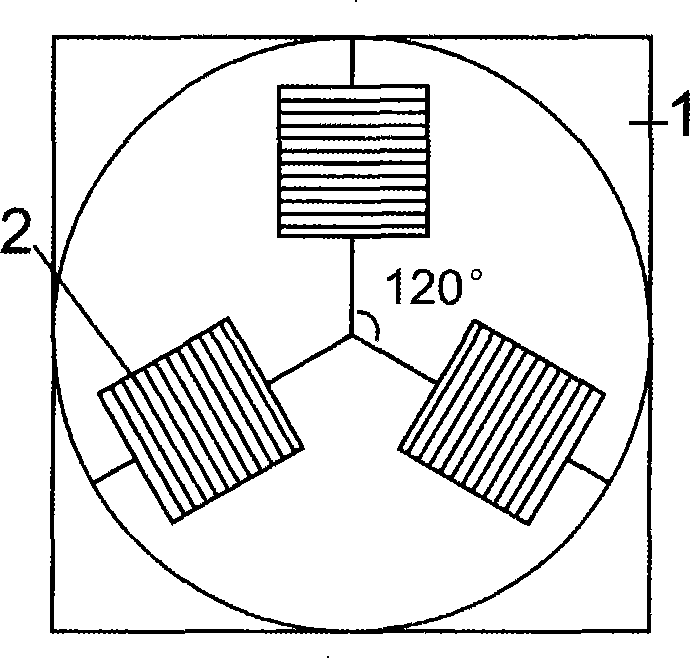
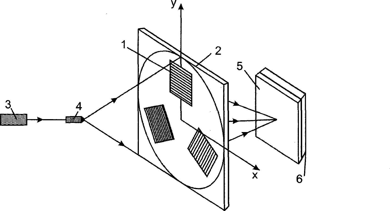
[0027] see figure 1 and 2 , the laser light output by the laser 3 is projected on the holographic optical element 1 after being expanded by the spatial filter 4 . Holographic optical elements 1 such as figure 1 As shown, it is made by holography and consists of three groups of identical holographic gratings 2 with 120° symmetry. When the expanded laser beam is vertically projected onto the holographic optical element 1, due to the action of the three sets of diffraction gratings, the holographic optical element 1 diffracts three sets of diffracted light, which converge on the central optical axis at the same angle, and the interference pattern is similar to Lattice structure in hexagonal crystals. The recording material is placed in the area where the three beams of diffracted light overlap and interfere, and the hexagonal periodic microstructure pattern can be recorded after exposure.

[0028] The laser adopts argon ion laser (wavelength 458nm), which is determined by the...

Embodiment 2

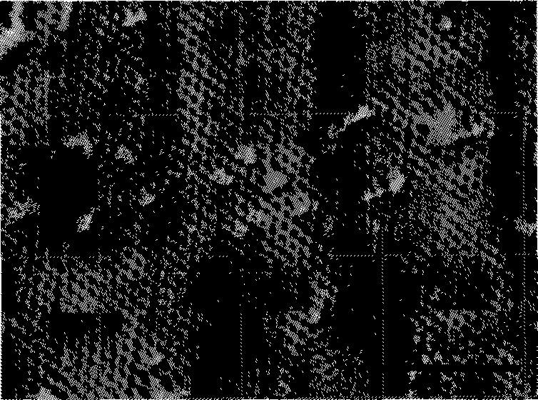
[0035] Similar to Example 1, the difference is that the angle between the three beams of light is adjusted to be 8.78°, and the microscopic photo of polysilicon etched with a period of 2 μm microstructure pattern is obtained. Figure 4 .

Embodiment 3

[0037] Similar to Example 1, the difference is that the angle between the three beams of light is adjusted to be 5.67°, and the microscopic photo of polysilicon etched with a microstructure pattern with a period of 3.09 μm is obtained. Figure 5 .


PUM


Abstract

The present invention provides a polysilicon solar cell texture layer preparation method, relating to a solar cell, in particular to a polysilicon solar cell anti-reflection layer manufacturing process which utilizes a laser holographic method and is combined with a wet etching method. The present invention provides a polysilicon solar cell texture layer preparation method which is used for the fast manufacturing of large-area periodic microstructures, and has low cost as well as good anti-reflection effect. The preparation method comprises the following steps that: a polysilicon silicon chip is pretreated; holographic recording is carried out to a photoresist material on the surface of the polysilicon silicon chip for manufacturing two-dimensional periodic microstructure; with the photoresist as a structure template, a structure is manufactured into a silicon material by adopting acidic corrosive liquid.

Description

technical field [0001] The invention relates to a solar cell, in particular to a process for manufacturing a textured anti-reflection layer of a polycrystalline silicon solar cell using a laser holography method combined with a wet etching method. Background technique [0002] Texture technology is a surface treatment process that reduces surface reflectivity and improves light absorption, and is generally used in the production of polycrystalline silicon solar cells. Due to the disordered crystal orientation of polycrystalline silicon, it is impossible to obtain a pyramid-like surface structure through anisotropic etching to reduce reflectivity like monocrystalline silicon. Therefore, it is necessary to simply and effectively perform anti-reflection treatment on the surface to improve the photoelectric conversion efficiency of polycrystalline silicon solar cells. . [0003] The existing texture technology mainly includes the following methods: 1) mechanical etching (see li...

Claims


Application Information

Patent Timeline
Patent Type & Authority Applications(China)
IPC IPC(8): H01L31/18
CPCY02P70/50
Inventor 陈小韵刘守张向苏任雪畅
Owner XIAMEN UNIV
Learn More