
Method for making nano-groove on quartz glass

A technology of quartz glass and a manufacturing method, which is applied in the direction of chemical instruments and methods, laboratory containers, and manufacturing microstructure devices, etc., can solve the problems of expensive processing costs, achieve rich sources, simple processing processes, and good micro-processing effect of nature

Inactive Publication Date: 2011-09-21
SHANGHAI INST OF MICROSYSTEM & INFORMATION TECH CHINESE ACAD OF SCI
View PDF0 Cites 0 Cited by
  • Summary
  • Abstract
  • Description
  • Claims
  • Application Information

AI Technical Summary

Problems solved by technology

Special reaction equipment is required and different flow rates of reaction gases need to be prepared according to different materials, and the processing cost is expensive

Method used


Image

  • Method for making nano-groove on quartz glass
  • Method for making nano-groove on quartz glass

Examples


Embodiment 1

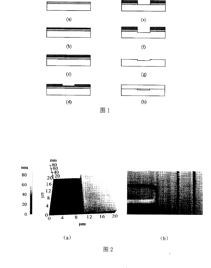
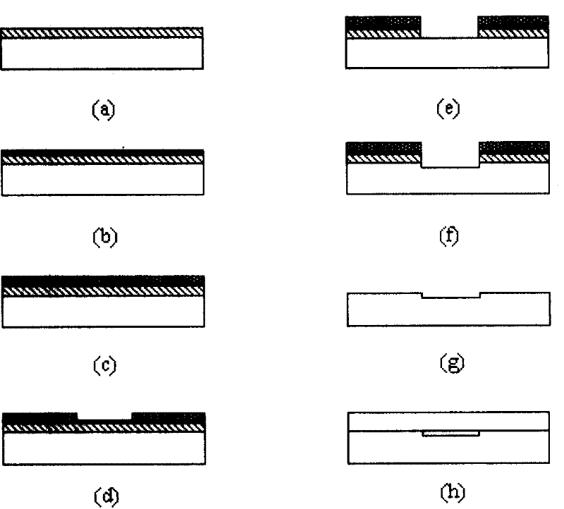
[0028] Fabricate 50nm nanochannels between microtubes.

[0029] 1) First photolithography

[0030] 1. Cleaning: Use acetone, ethanol and deionized water to ultrasonically clean the substrate for 5 minutes; blow dry with nitrogen; dry (120°C) for 20 minutes

[0031] 2. Evaporate organosilicon oxide (HMDS); apply 6809 photoresist, and shake the glue at 4000rpm for 30s

[0032] 3. Pre-baking: 100℃, 6min

[0033] 4. Photolithography: the use intensity is 12mW / cm 2 Lithography machine, Lithography 12s

[0034] 5. Development: 18s

[0035] 6. Base film 10S

[0036] 7. Harden the film in an oven at 120°C for 30 minutes

[0037] 2) Main pipeline corrosion

[0038] 1. Chromium removal: Use chromium corrosion solution (cerium ammonium nitrate 400g + perchloric acid 110mL, deionized water to 1.76L) to remove the chromium layer of the graphic part

[0039] 2. Wash with deionized water 10 times

[0040] 3. Glass corrosion: put in 40-50℃ constant temperature quartz glass corrosion ...

Embodiment 2

[0063] Fabricate a "m"-shaped 100nm nanochannel chip.

[0064] 1) Photolithography (nanostructure)

[0065] 1. Cleaning: Use acetone, ethanol, and deionized water to ultrasonically clean the substrate for 5 minutes; blow dry with nitrogen; dry (120°C) for 20 minutes

[0066] 2. Spin glue, photoresist 6809 4000rpm, 30s thickness: 0.9μm

[0067] 3. Pre-baking: 100°C, 6min (hot plate)

[0068] 4. Alignment photolithography: use an intensity of 12mW / cm 2 Lithography machine Lithography 12s

[0069] 5. Development: 18s

[0070] 6. Base film 10S

[0071] 7. Harden the film in an oven at 120°C for 30 minutes

[0072] 2) Fabrication of nanopipes

[0073] 1. Chromium removal: Use chromium corrosion solution (cerium ammonium nitrate 400g + perchloric acid 110mL, deionized water to 1.76L) to remove the chromium layer of the graphic part

[0074] 2. Nano-corrosion: put in 40-50℃ constant temperature quartz glass corrosion solution (HF:H 2 o 2 :HAC=2:5:5, volume ratio) stirring, ...


PUM

PropertyMeasurementUnit
thicknessaaaaaaaaaa

Abstract

The invention relates to a nano-channel preparing method on a piece of quartz glass, characterized in that the crucial technology for preparing comprises three steps of photoetching, wet etching and linking, wherein the wet etching solution preparation is one of the crucial steps of the MEMS processing technology, and can directly influence the graphic structure of the nano-channels. The invention employs the quartz glass as the substrate material, the technology is simple and has no need of reactive ion etching equipment, and the depth error of the nano-channel can be precisely controlled tobe + / -1nm or so by regulating the etching time and temperature on the basis of the prepared etching solution.

Description

technical field [0001] The invention relates to a method for manufacturing a nanometer channel on quartz glass, which belongs to the technical field of microprocessing. Background technique [0002] Micro total analytical system (μTAS), also known as Lab-on-a-chip (Lab-on-a-chip), was a concept proposed by Manz et al. in the 1990s. systems, MEMS) and analytical chemistry detection, the basic operation units involved in the fields of biology and chemistry, such as sample preparation, biological and chemical reactions, separation, detection, etc. are integrated or basically integrated into a chip of a few square centimeters. It is a technology to complete different biological or chemical reaction processes and analyze their products. After more than ten years of development, the separation, analysis and detection systems of nucleic acids, proteins, organic compounds and inorganic ions on microchips have developed rapidly, and integrated commercial micro-total analysis systems...

Claims


Application Information

Patent Timeline
Patent Type & Authority Patents(China)
IPC IPC(8): B81C1/00C03C15/00B01J19/00B01L3/00G01N35/00
Inventor 金庆辉刘菁赵建龙
Owner SHANGHAI INST OF MICROSYSTEM & INFORMATION TECH CHINESE ACAD OF SCI
Learn More