
Methods of forming reverse side engineered III-nitride devices

Active Publication Date: 2016-11-15
TRANSPHORM INC
View PDF253 Cites 7 Cited by
  • Summary
  • Abstract
  • Description
  • Claims
  • Application Information

AI Technical Summary

Benefits of technology

The patent text describes a technique for making high voltage lateral group III nitride devices. This can be done by fabricating a semiconductor stack on a low cost substrate and then removing it after attaching it to a carrier wafer with metallization and vias. The substrate can also be thinned and defects can be removed from the reverse surface. The device can be made more accessible by adding appropriate vias and metallization to the reverse. The technical effect of this technique is to provide a cost-effective way to make high voltage lateral group III nitride devices with improved performance and reliability.

Problems solved by technology

However, applications have been hampered by a lack of low cost substrates for device fabrication.
It can be difficult to grow thick gallium nitride by heteroepitaxy.
Thus, high voltage lateral devices require large areas and need to be made on low cost substrates.
However, due to the large lattice and thermal mismatch between silicon and gallium nitride, nucleation and stress management layers may be required.
While this approach can produce acceptable spacer, channel and barrier layers, a high quality thick buffer layer is difficult to achieve.
Because the layers below the spacer layer can have a high concentration of defect levels in the bandgap, this can cause drain voltage induced current collapse and leakage at high drain biases and can also reduce breakdown voltage of the device.

Method used


Image

  • Methods of forming reverse side engineered III-nitride devices
  • Methods of forming reverse side engineered III-nitride devices
  • Methods of forming reverse side engineered III-nitride devices

Examples


Embodiment Construction

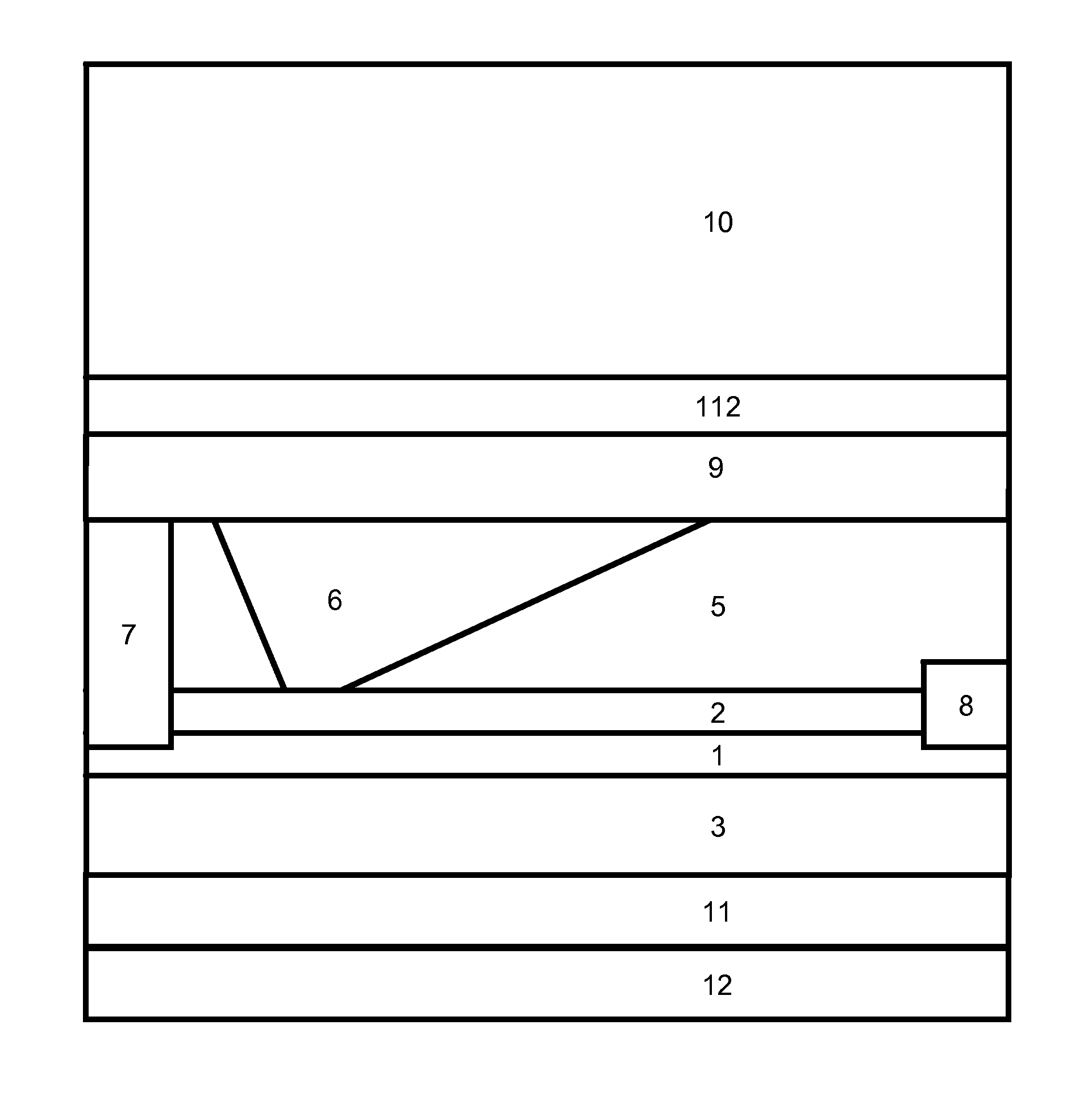
[0021]Described herein are techniques that enable III-nitride type devices to be formed using silicon base substrates.

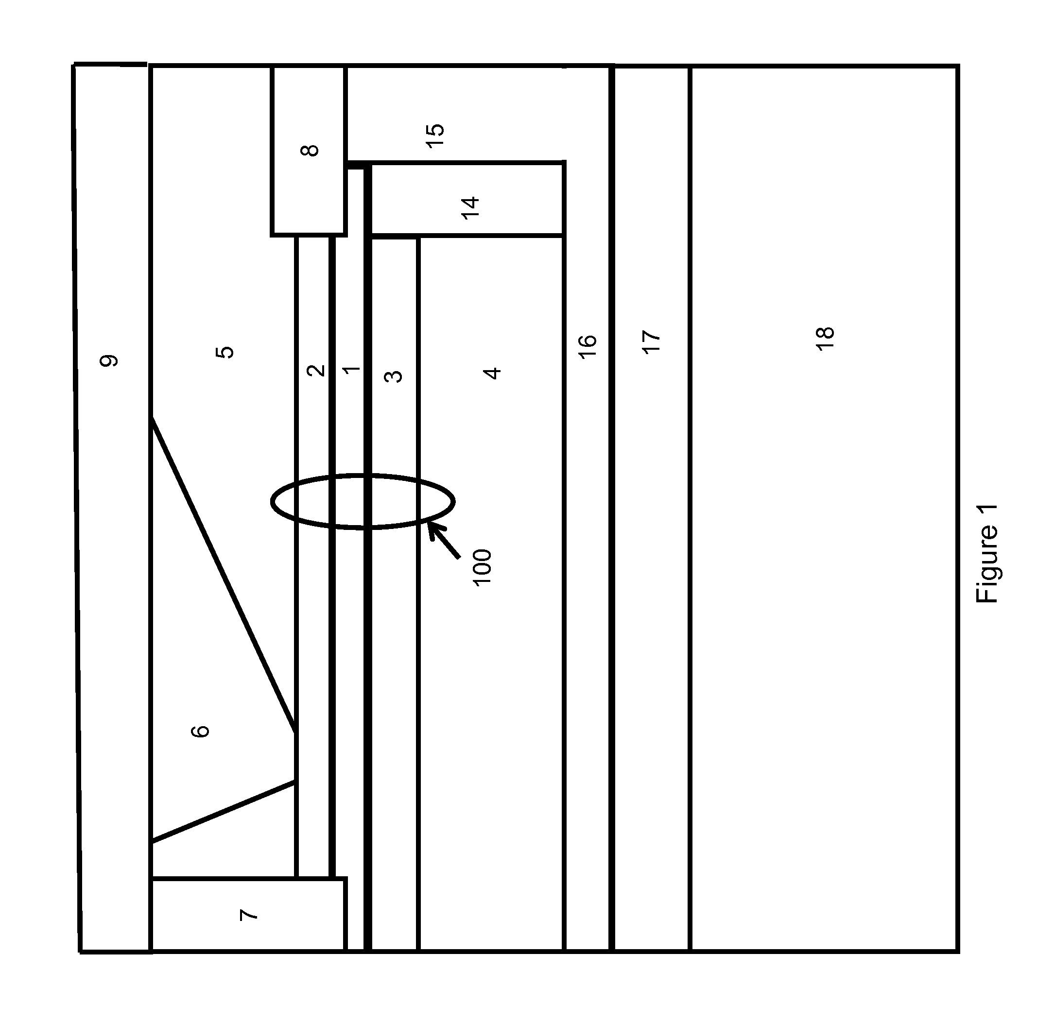
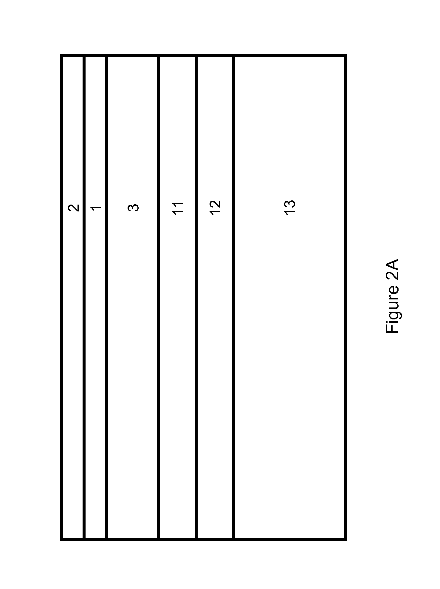
[0022]As used herein the obverse or device face is the face of the wafer or epitaxial layer on which a lateral device is fabricated by forming electrodes that make ohmic and / or Schottky and / or metal-insulator-semiconductor (MIS) contacts to the semiconductor. The reverse face is opposite to the obverse or device face. As used herein, the term “III-nitride material” or “III-N material” refers to a compound semiconductor material according to the stoichiometric formula AlxInyGazN, where x+y+z is equal to 1 or about 1. The devices described herein are group III face devices. However, the techniques described herein can be applied to N-face devices with the appropriate change in the relative location of the 2DEG layer and layer type (i.e., whether the layer is p- or n-type or intrinsic). As used herein, “active layer(s)” are a set of III-nitride layers in which devices a...


PUM


Abstract

Group III-nitride devices are described that include a stack of III-nitride layers, passivation layers, and conductive contacts. The stack includes a channel layer with a 2DEG channel, a barrier layer and a spacer layer. One passivation layer directly contacts a surface of the spacer layer on a side opposite to the channel layer and is an electrical insulator. The stack of III-nitride layers and the first passivation layer form a structure with a reverse side proximate to the first passivation layer and an obverse side proximate to the barrier layer. Another passivation layer is on the obverse side of the structure. Defected nucleation and stress management layers that form a buffer layer during the formation process can be partially or entirely removed.

Description

CROSS-REFERENCE TO RELATED APPLICATION[0001]This is a divisional of U.S. Application Ser. No. 12 / 635,405, filed on Dec. 10, 2009 (now U.S. Pat. No. 8,389,977), the disclosure of which is considered part of and is incorporated by reference in the disclosure of this application.TECHNICAL FIELD[0002]This invention relates to semiconductor devices fabricated on group III-nitride semiconductors.BACKGROUND[0003]Group III-nitride based devices have many potential material advantages over silicon based devices for high power electronics applications. Amongst others, these include larger bandgap and breakdown field, high electron mobility in a two dimensional electron gas (2DEG), low thermal generation current, and the possibility of using the direct bandgap plus a great variety of band and polarization engineering techniques applicable in many of these structures for novel device functions. However, applications have been hampered by a lack of low cost substrates for device fabrication.[000...

Claims


Application Information

Patent Timeline
IPC IPC(8): H01L29/06H01L21/02H01L29/417H01L29/66H01L29/778H01L29/423H01L29/20H01L23/31H01L23/29H01L23/00
CPCH01L21/0254H01L29/4175H01L29/66462H01L29/7786H01L23/291H01L23/3171H01L24/03H01L24/06H01L29/2003H01L29/42316H01L2224/03002H01L2224/03462H01L2224/03464H01L2224/04042H01L2224/06183H01L2224/94H01L2924/01029H01L2924/1032H01L2924/12032H01L2924/12042H01L2924/13062H01L2924/13064H01L2224/03H01L2924/00H01L29/6609H01L29/861
Inventor CHU, RONGMINGMISHRA, UMESHLAL, RAKESH K.
Owner TRANSPHORM INC
Learn More