Piezoelectric thin film element
a thin film element and piezoelectric technology, applied in the direction of electrical equipment, metallic material coating process, device material selection, etc., can solve the problems of unfavorable ferroelectric characteristics, unfavorable leakage current characteristics, rapid increase of leakage current, etc., to achieve excellent leakage current characteristics, ferroelectric characteristics, and piezoelectric characteristics.
- Summary
- Abstract
- Description
- Claims
- Application Information
AI Technical Summary
Benefits of technology
Problems solved by technology
Method used
Image
Examples
first embodiment
Manufacture of Piezoelectric Thin Film Element
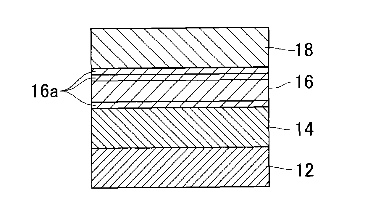
[0035]FIG. 2 is a cross-sectional view schematically illustrating the configuration of a piezoelectric thin film element according to a first embodiment. The piezoelectric thin film element includes a substrate 12, a lower electrode 14 formed on the substrate 12, a piezoelectric thin film 16 formed on the lower electrode 14, and an upper electrode 18 formed on the piezoelectric thin film 16.
[0036]It is to be noted that the content of BaZrO3 in a potassium sodium niobate thin film represented by the general formula (1−n)(K1-xNax)NbyO3-nBaZrO3 as the piezoelectric thin film 16 is varied in the first embodiment.
[0037]For example, a silicon substrate (Si substrate) is used for the substrate 12. Further, for the substrate 12, substrates may be used such as a glass substrate, a quartz glass substrate, a GaAs substrate, a GaN substrate, a CaF2 substrate, a sapphire substrate, an MgO substrate, an SrTiO3 substrate, an LaAlO3 substrate, a stainle...
second embodiment
Manufacture of Piezoelectric Thin Film Element
[0066]A piezoelectric thin film element according to a second embodiment is configured in the same fashion as the piezoelectric thin film element shown in FIG. 2 according to the first embodiment.
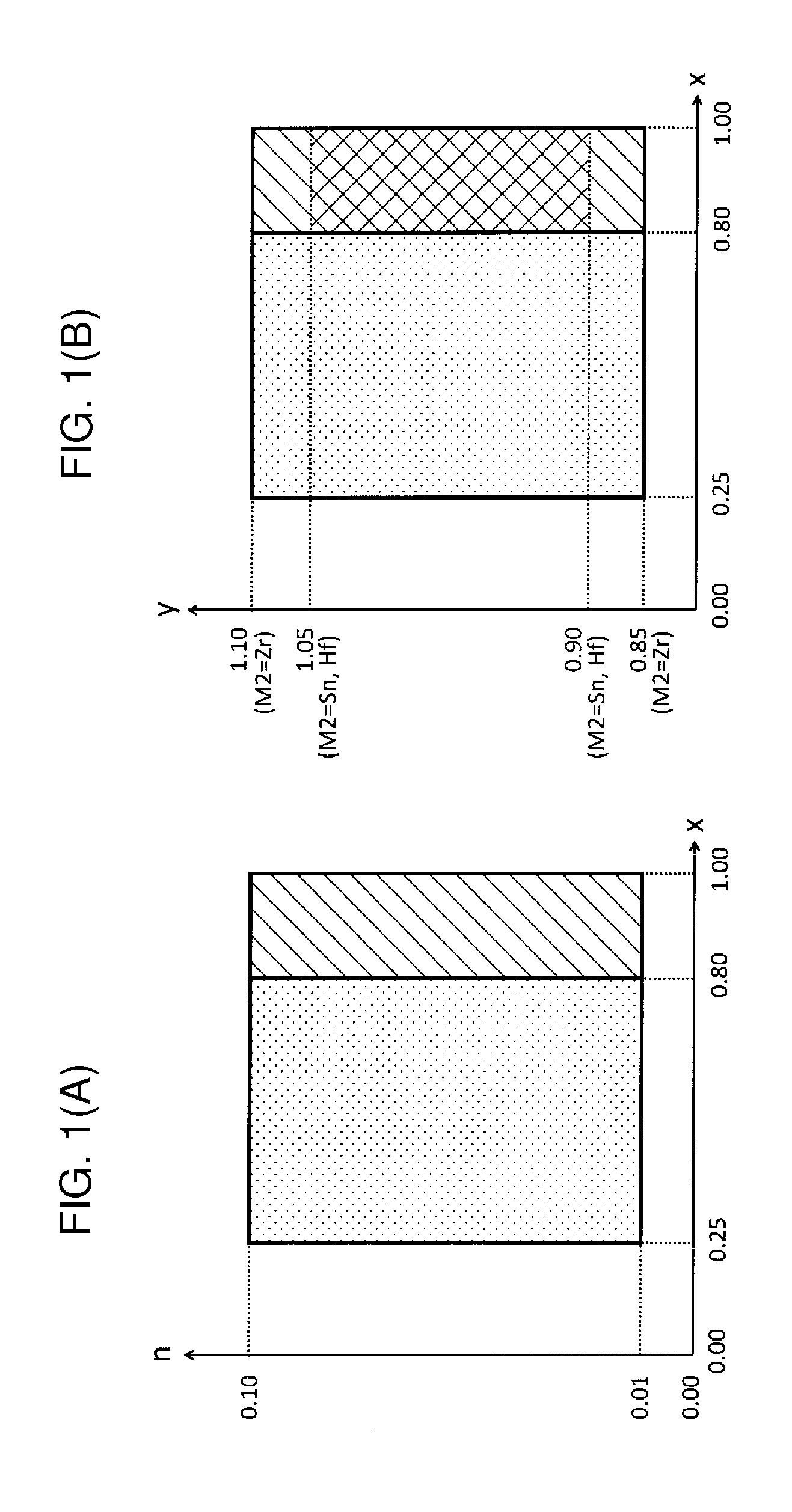
[0067]It is to be noted that the x and y in a potassium sodium niobate thin film represented by the general formula (1−n)(K1-xNax)NbyO3-nBaZrO3 as the piezoelectric thin film 16 are varied in the second embodiment.
[0068]The piezoelectric thin film 16, that is, potassium sodium niobate (KNN) thin film 16 is created by using a chemical solution deposition method.
[0069]First, potassium ethoxide, sodium ethoxide, pentaethoxy niobium, manganese acetylacetonato, barium ethoxide (or calcium ethoxide or strontium ethoxide), and tetraisopropoxy zirconium as raw materials are prepared to meet (1.07−x)×0.97:(x+0.17)×0.97:y×0.97:0.02×0.97:0.03:0.03 in terms of molar ratio. In the case of the present second embodiment herein, x and y respectively satisfy a c...
third embodiment
Manufacture of Piezoelectric Thin Film Element
[0107]A piezoelectric thin film element according to a third embodiment is configured in the same fashion as the piezoelectric thin film element shown in FIG. 2 according to the first embodiment.
[0108]It is to be noted that the content of BaSnO3 in a potassium sodium niobate thin film represented by the general formula (1−n)(K1-xNax)NbyO3-nBaSnO3 as the piezoelectric thin film 16 is varied in the third embodiment.
[0109]The piezoelectric thin film 16, that is, potassium sodium niobate (KNN) thin film 16 is created by using a chemical solution deposition method.
[0110]First, potassium ethoxide, sodium ethoxide, pentaethoxy niobium, manganese acetylacetonato, barium ethoxide, and tetraisopropoxy tin as raw materials are prepared to meet 0.52×(1−n): 0.72×(1−n): 0.95×(1−n): 0.02×(1−n): n:n in terms of molar ratio. In the case of the present third embodiment herein, seven types of 0.00, 0.005, 0.01, 0.03, 0.05, 0.1, and 0.12 are selected as n.
[...
PUM
| Property | Measurement | Unit |
|---|---|---|
| thickness | aaaaa | aaaaa |
| grain size | aaaaa | aaaaa |
| electric field | aaaaa | aaaaa |
Abstract
Description
Claims
Application Information
 - R&D
- Intellectual Property
- Life Sciences
- Materials
- Tech Scout
- Unparalleled Data Quality
- Higher Quality Content
- 60% Fewer Hallucinations
Browse by: Latest US Patents, China's latest patents, Technical Efficacy Thesaurus, Application Domain, Technology Topic, Popular Technical Reports.
© 2025 PatSnap. All rights reserved.Legal|Privacy policy|Modern Slavery Act Transparency Statement|Sitemap|About US| Contact US: help@patsnap.com


