
Method for treating a semiconductor

a technology of semiconductors and layers, applied in the field of methods for treating semiconductor layers, can solve the problems of high back contact resistance, low power conversion efficiency of cdte-based photovoltaic devices, and high work function of cd

Active Publication Date: 2016-06-21
FIRST SOLAR INC
View PDF2 Cites 2 Cited by
  • Summary
  • Abstract
  • Description
  • Claims
  • Application Information

AI Technical Summary

Benefits of technology

This approach results in more efficient and stable photovoltaic devices with improved carrier concentration and reduced defects, maintaining consistent performance and long-term stability by forming deeper chalcogen-rich regions and optimizing dopant distribution.

Problems solved by technology

However, CdTe-based photovoltaic devices typically demonstrate relatively low power conversion efficiencies, which may be attributed to a relatively low open circuit voltage (Voc) in relation to the band gap of the material which is due, in part, to the low effective carrier concentration and short minority carrier lifetime in CdTe.
Further issues with improving the device efficiency of CdTe solar cells include the high work function of CdTe and high back-contact resistance at the interface between CdTe and metal-based back contact layer.
However, it may be difficult to control the amount of copper incorporated in the bulk and in the back interface, using a typical CdTe processing method.
Further, photovoltaic devices manufactured using the typical methods may include a high copper content at the back-interface, which may adversely affect the long-term stability.
Furthermore, etching of the CdTe layer using conventional etching agents may lead to removal of CdTe material from the surface, and selective etching of grain boundaries, resulting in increased defects.

Method used


Image

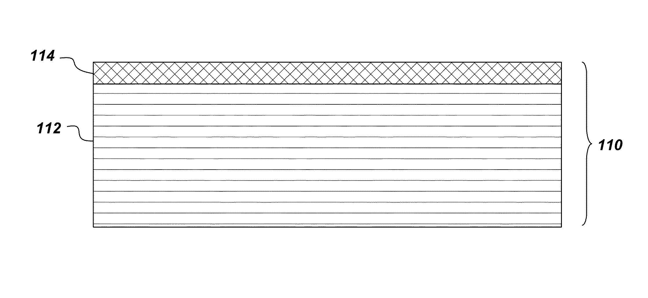
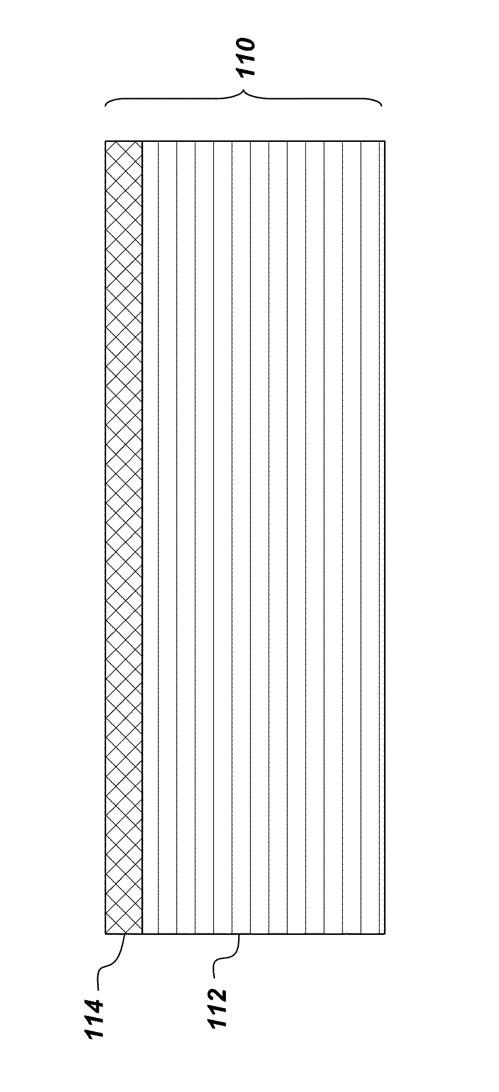
  • Method for treating a semiconductor
  • Method for treating a semiconductor

Examples


example 1

[0046]A chemical agent paste was prepared by mixing 1 gram of fumed silica (0.2-0.3 micrometers diameter), 5 grams of propylene glycol, and 1 drop of a solution containing 1.0 molar elemental iodine in 1.0 molar potassium iodide. The paste was applied by brush coating onto cadmium telluride samples. The coated samples were heated on a hot plate for 2 minutes, and then the paste was removed with a water rinse. The paste did not lose its ability to wet the surface of the samples as the exposure occurred, in contrast to behavior observed for aqueous compositions. The paste remained orange colored, indicating that iodine was present throughout the exposure. A tellurium-enriched region was observed to form on the exposed area of the samples.

example 2

[0047]Thin film photovoltaic devices were fabricated using cadmium telluride (CdTe) as the absorber layer. The CdTe layer of the devices, after deposition, were treated with a paste chemical agent made by mixing 8 grams of fumed silica, 50 grams of propylene glycol, and 0.5 ml of iodine solution (1.0 moles / liter potassium iodide plus 0.5 moles / liter elemental iodine). Various devices were respectively subjected to one of several time-temperature combinations, with times ranging from 2 minutes to 20 minutes and temperatures ranging from 65 degrees Celsius to 150 degrees Celsius. A control group was treated using an immersion process in an aqueous iodine solution. After treatment with the iodine-containing chemical agent, fabrication of the devices was completed and then the resultant devices were tested in highly accelerated life tests (HALT). Several of the experimentally processed devices exhibited comparable performance to that of the control devices. Devices made with shorter exp...


PUM

PropertyMeasurementUnit
boiling pointaaaaaaaaaa
temperatureaaaaaaaaaa

Abstract

Methods for treating a semiconductor material, and for making devices containing a semiconducting material, are presented. One embodiment is a method for treating a semiconductor material that includes a chalcogenide. The method comprises contacting at least a portion of the semiconductor material with a chemical agent. The chemical agent comprises a solvent, and an iodophor dissolved in the solvent.

Description

RELATED APPLICATIONS[0001]This application claims priority from U.S. nonprovisional application Ser. No. 13 / 682,876, filed Nov. 21, 2012, pending and bearing the title “METHODS FOR TREATING A SEMICONDUCTOR.” The above-mentioned nonprovisional application is incorporated herein by reference in its entirety.BACKGROUND[0002]The invention generally relates to methods for treating a semiconductor material. More particularly, the invention relates to methods for treating a semiconductor layer used in thin-film photovoltaic devices.[0003]Thin film photovoltaic devices typically include a plurality of semiconductor layers disposed on a transparent substrate, wherein a first semiconductor layer serves as a window layer and a second semiconductor layer serves as an absorber layer. The window layer allows the penetration of solar radiation to the absorber layer, where the optical energy is converted to usable electrical energy. In certain configurations, thin film photovoltaic devices may furt...

Claims


Application Information

Patent Timeline
Patent Type & Authority Patents(United States)
IPC IPC(8): H01L31/0445H01L31/0224H01L31/18H01L31/0475H01L31/073H01L31/0296
CPCH01L31/1828H01L31/02963H01L31/022425H01L31/0445H01L31/0475H01L31/073Y02E10/543Y02P70/521H01L21/02562H01L21/02581H01L21/02664Y02P70/50
Inventor FOUST, DONALD FRANKLIN
Owner FIRST SOLAR INC
Learn More