
Silicon single crystal doped with gallium, indium, or aluminum

a single crystal, gallium-based technology, applied in the direction of conductors, packaging goods, foodstuffs, etc., can solve the problems of ingots with the desired resistivity, lower dopant concentration, higher resistivity, etc., to achieve uniform radial and axial resistivity, reduce downtime, and reach the steady state more quickly

Active Publication Date: 2015-06-09
GTAT IP HLDG
View PDF78 Cites 7 Cited by
  • Summary
  • Abstract
  • Description
  • Claims
  • Application Information

AI Technical Summary

Benefits of technology

The invention relates to a process for growing silicon single crystals with uniform electrical properties. The process involves adding a dopant, such as gallium, aluminum, or indium, to the initial silicon charge or the melt between crystal ingot growth using a sacrificial vessel. This helps to speed up the system's steady-state and results in more uniform resistivity at the seed end. Dopant can also be added continuously or semi-continuously during crystal growth using silicon-dopant alloy cubes or containers made of silicon. These containers can be added without the dopant melting and sticking to the feed apparatus.

Problems solved by technology

This is difficult to achieve due, in part, to segregation.
A doped batch CZ process potentially results in an ingot having the desired resistivity in only a small portion of the ingot.
One problem that continues to persist during a CCZ run is the tendency for dopant to migrate or diffuse to the outer melt zone of the crucible (due to the concentration gradient), which results in lower dopant concentration and higher resistivity at the seed end of the next crystal ingot until the steady state can be achieved again.
It has been recognized, however, that boron forms recombination active defects with oxygen under illumination thereby lowering the minority carrier lifetime.
This effect known as “light induced degradation” or “LID” causes a significant voltage and current drop of the solar cells when in operation.
This lack of uniformity increases the cost of production due to the limited amount of acceptable material in each ingot and / or the cost of development of cell manufacturing processes that can accommodate material exhibiting a wide resistivity range.
This is likely due to the fact that elemental gallium (the most preferred of the three dopants) would be difficult to add in a sufficiently high concentration using a continuous or semi-continuous feeding apparatus because it melts near room temperature and would stick to the apparatus.
This not only has the potential of damaging the apparatus, but also creates operational problems such as a lack of control of the actual amount of gallium being added to the melt.
In addition, gallium forms a highly volatile suboxide (Ga2O) that results in significant loss of gallium from the melt due to evaporation.

Method used


Image

  • Silicon single crystal doped with gallium, indium, or aluminum
  • Silicon single crystal doped with gallium, indium, or aluminum
  • Silicon single crystal doped with gallium, indium, or aluminum

Examples


example 1

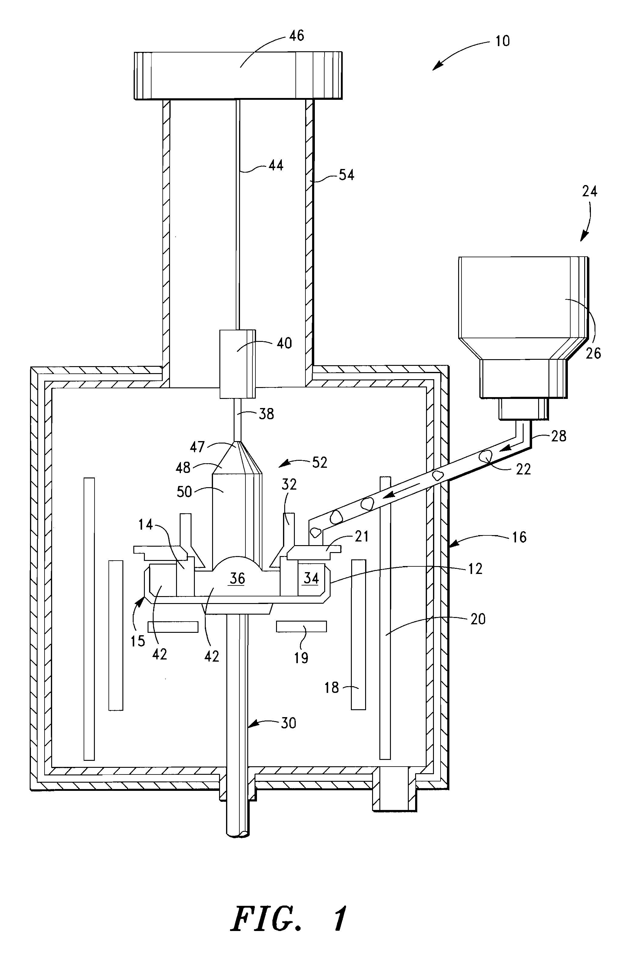
[0062]In FIG. 15, the radial resistivity of a crystal ingot (sample 1) made in accordance with the preferred embodiment of this invention is shown. The crystal was the third ingot grown in a CCZ run wherein elemental gallium was added in the initial charge and within the growth zone 36 via a cup-like vessel formed on seed crystal 38 between ingots in an amount determined in accordance with the doping model. No additional dopant was added into the melt zone 34 during crystal growth or between ingot growth. As can be seen, the radial resistivity is relatively uniform throughout the length of the crystal. It is noted that the resistivity measurements for all examples were taken post thermal donor kill or TDK, a heat treatment that is applied to silicon wafers so that their measured resistivity better reflects actual working resistivities for use in solar cells. FIG. 16 shows the resistivity of the crystal sample 1 along the axial length of sample 1.

example 2

[0063]FIG. 17 shows the actual amount of gallium dopant added to three crystal ingots produced using the CCZ process and in accordance with the doping model of the present invention. The amount of dopant added inter-ingot was determined in accordance with the doping model and based upon the desired resistivity of the ingot. No additional dopant was added in the outer chamber during or between ingot growth. FIG. 17 shows the anticipated resistivity in accordance with the model and the actual measured resistivity.

[0064]FIG. 18 shows the actual resistivity of the three crystals grown and shown in preceding FIG. 17 along the length of each crystal. FIG. 19 shows the axial resistivity of crystals grown with both gallium doping in the inner growth chamber between ingot growth and additional dopant added during growth to the outer chamber by means of dopant containers, in comparison to a crystal with doping only to the inner growth chamber between ingot growth. It is noted that the resisti...

example 3

[0065]For this experiment, 40 solar cells were made from 125 mm×125 mm pseudo-square wafers. Next to a control group of 10 wafers for the optimization, 15 cells were made of boron doped substrates using a CCZ process with addition of dopant to the inner growth chamber between ingot growth and addition to the outer growth chamber during growth, and 15 cells were made of gallium doped substrates with addition of dopant to the inner growth chamber between ingot growth. The resistivities of the wafers are given in Table I. Note that Group 2 has approximately double the dopant concentration compared to Group 1.

[0066]

TABLE IResistivities of the used substrates.Base dopingResistivityGroup 1p-type, Boron2.1 Ω cmGroup 2p-type, Gallium1.0 Ω cm

[0067]With reference to FIG. 20, the solar cell process used in this experiment was a selective emitter approach adhering closely to standards used in the industry. The cells underwent an alkaline texturing before POCl3 emitter diffusion to about 30 Ω / sq...


PUM

PropertyMeasurementUnit
resistivityaaaaaaaaaa

Abstract

A doped silicon single crystal having a resistivity variation along a longitudinal and / or radial axis of less than 10% and a method of preparing one or a sequential series of doped silicon crystals is disclosed. The method includes providing a melt material comprising silicon into a continuous Czochralski crystal growth apparatus, delivering a dopant, such as gallium, indium, or aluminum, to the melt material, providing a seed crystal into the melt material when the melt material is in molten form, and growing a doped silicon single crystal by withdrawing the seed crystal from the melt material. Additional melt material is provided to the apparatus during the growing step. A doping model for calculating the amount of dopant to be delivered into the melt material during one or more doping events, methods for delivering the dopant, and vessels and containers used to deliver the dopant are also disclosed.

Description

CROSS-REFERENCE TO RELATED APPLICATIONS[0001]This application is based on and claims priority to U.S. Provisional Patent Application Ser. No. 61 / 402,776 filed on Sep. 3, 2010.STATEMENT REGARDING FEDERALLY SPONSORED RESEARCH OR DEVELOPMENT[0002]Not applicable.FIELD OF THE INVENTION[0003]This invention generally relates to single crystal ingots grown using the batch and continuous Czochralski methods and is more specifically directed to silicon single crystal ingots doped with gallium, indium and / or aluminum and methods of making and using the same.BACKGROUND OF THE INVENTION[0004]Several processes are known in the art for growing crystal ingots of semi-conductor materials for use in fabricating integrated circuits and photovoltaic devices such as solar cells. Batch and continuous Czochralski (“CZ”) processes are widely used for semiconductor materials such as silicon, germanium, or gallium arsenide doped with an elemental additive such as phosphorus (n-type dopant) or boron (p-type d...

Claims


Application Information

Patent Timeline
Patent Type & Authority Patents(United States)
IPC IPC(8): C30B15/04C30B29/06C30B15/00
CPCC30B15/04C30B29/06C30B15/002Y02E10/547C30B15/00C30B15/02H01L31/042
Inventor DELUCA, JOHN P.DELK, II, FRANK S.JOHNSON, BAYARD K.LUTER, WILLIAM L.MIDDENDORF, NEIL D.WILLIAMS, DICK S.OSTROM, NELS PATRICKHIGHFILL, JAMES N.
Owner GTAT IP HLDG
Learn More