System for producing patterned silicon carbide structures
- Summary
- Abstract
- Description
- Claims
- Application Information
AI Technical Summary
Benefits of technology
Problems solved by technology
Method used
Image
Examples
examples
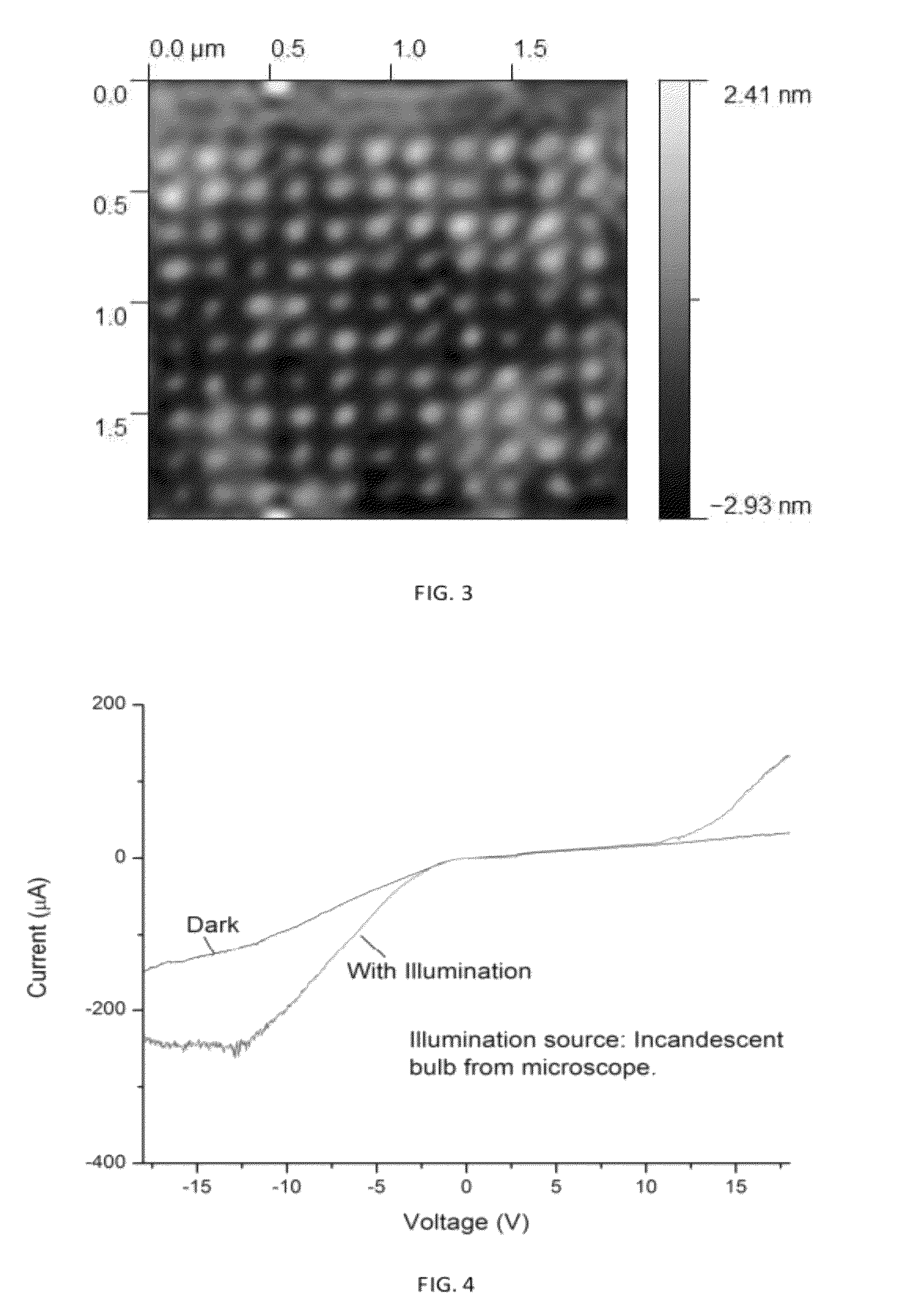
[0039]For these experiments, electron beam lithography was used to form arrays of nanowires as well as more complicated patterns. PMMA was spin coated on silicon substrates to a thickness of 200 nm. The patterns were created using a JEOL JSM 1401F field emission scanning electron microscope (SEM) using the NPGS nanopatterning system. Following electron beam exposure, the resist was developed in a 3:1 mixture of isopropyl alcohol and methyl isobutyl ketone (MIBK). This mixture produces the highest resolution patterns. Previous lithography tests with this SEM have shown a minimum pattern linewidth of 50 nm in 200 nm PMMA.
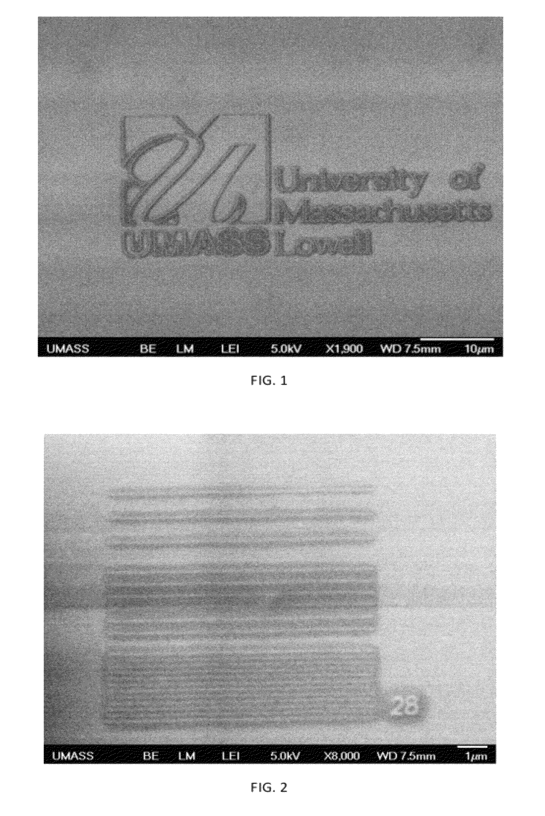
[0040]Patterns that were tested consisted of arrays of lines and dots with widths / diameters ranging from 50 nm to 500 nm. Several complex patterns with numerous curved shapes, such as the University of Massachusetts Lowell logo were also tried (FIG. 1). To assess the ability to form large areas with a uniform SiC film, a pattern with a width of 20 μm and a length of 1...
PUM
| Property | Measurement | Unit |
|---|---|---|
| Length | aaaaa | aaaaa |
| Thickness | aaaaa | aaaaa |
| Thickness | aaaaa | aaaaa |
Abstract
Description
Claims
Application Information
 - R&D Engineer
- R&D Manager
- IP Professional
- Industry Leading Data Capabilities
- Powerful AI technology
- Patent DNA Extraction
Browse by: Latest US Patents, China's latest patents, Technical Efficacy Thesaurus, Application Domain, Technology Topic, Popular Technical Reports.
© 2024 PatSnap. All rights reserved.Legal|Privacy policy|Modern Slavery Act Transparency Statement|Sitemap|About US| Contact US: help@patsnap.com


