Organic electroluminescent element, method for manufacturing the organic electroluminescent element, and light emitting display device
a technology of organic electroluminescent elements and electroluminescent elements, which is applied in the direction of thermoelectric device junction materials, electrical apparatus, and semiconductor devices, etc., can solve the problems of lowering the current density, lowering the luminescence characteristics, and ionizing electrons, so as to facilitate the injection of charges and reduce damage to the organic layer
- Summary
- Abstract
- Description
- Claims
- Application Information
AI Technical Summary
Benefits of technology
Problems solved by technology
Method used
Image
Examples
example 1
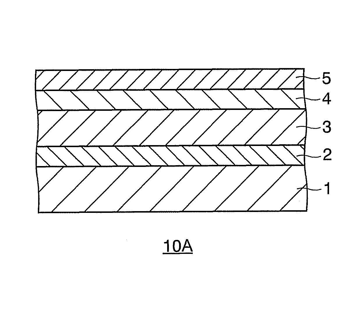
[0148]An ITO substrate was first provided. The ITO substrate had a 150 nm-thick line-patterned anode 2 of ITO (line width: 2 mm) provided on a transparent base material 1 formed of a glass substrate. TBADN represented by chemical formula 5 above and MoO3 as an oxidizing dopant were codeposited on the ITO substrate at a deposition rate of 1.5 angstroms / sec under a degree of vacuum of 10-5 Pa so that the weight ratio of TBADN to MoO3 was 67:33, thereby forming a 10 nm-thick hole injection layer.
[0149]TBADN represented by chemical formula 5 as described above was then vacuum-deposited on the hole injection layer at a deposition rate of 1.0 angstrom / sec under a degree of vacuum of 10-5 Pa to form a 10 nm-thick hole transport layer. The laminate composed of the hole injection layer and the hole transport layer can be said to be a hole injection / transport layer 3a having an oxidizing dopant-mixed region (hole injection layer) on the anode side.
[0150]TCTA represented by chemical formula 6 ...
example 2
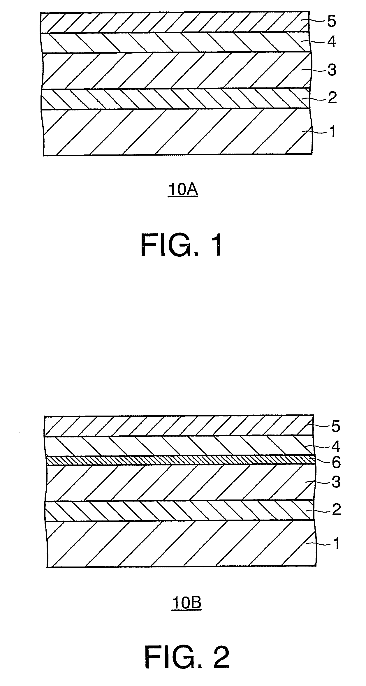
[0162]An organic EL element of Example 2 was prepared in the same manner as in Example 1, except that, in the organic EL element of Example 1, an electroconductive layer 6 of aluminum (thickness 2 nm) was formed between the electron injection / transport layer 3c and the transparent protective layer 4 at a deposition rate of 0.5 angstrom / sec under a degree of vacuum of 10-5 Pa. The organic EL element of Example 2 was observed under a scanning electron microscope. As a result, the formed 2 nm-thick Al was in an sea-island form.
example 3
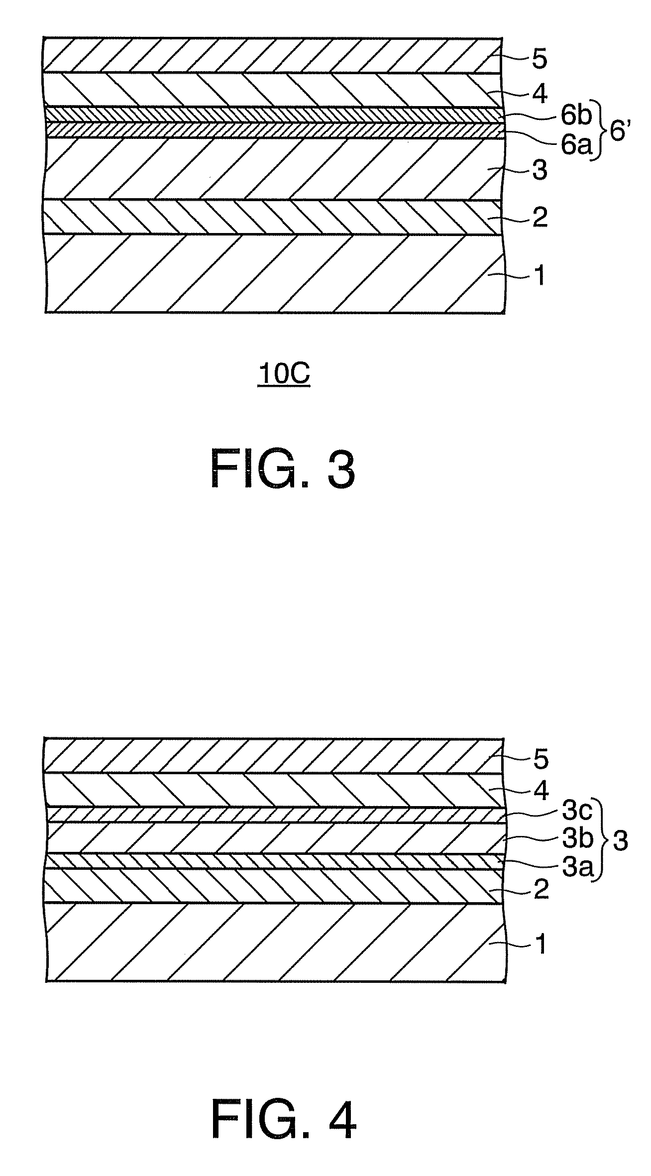
[0166]An organic EL element of Example 3 was prepared in the same manner as in Example 1, except that, in the organic EL element of Example 1, an electroconductive layer 6′ was provided between the electron injection / transport layer 3c and the transparent protective layer 4 by forming a first electroconductive layer 6a of Al (thickness 2 nm) from the electron injection / transport layer 3c side at a deposition rate of 0.5 angstrom / sec under a degree of vacuum of 10-5 Pa and further forming a second electroconductive layer 6b of MgAg (thickness 5 nm) on the first electroconductive layer 6a at a deposition rate of 1 angstrom / sec under a degree of vacuum of 10-5 Pa.
PUM
 Abstract
Description
Claims
Application Information
 - R&D
- Intellectual Property
- Life Sciences
- Materials
- Tech Scout
- Unparalleled Data Quality
- Higher Quality Content
- 60% Fewer Hallucinations
Browse by: Latest US Patents, China's latest patents, Technical Efficacy Thesaurus, Application Domain, Technology Topic, Popular Technical Reports.
© 2025 PatSnap. All rights reserved.Legal|Privacy policy|Modern Slavery Act Transparency Statement|Sitemap|About US| Contact US: help@patsnap.com


