
Reduction of reactive gas attack on substrate heater

a technology for reducing reactive gas attack and substrate heater, which is applied in the direction of cleaning hollow articles, coatings, chemistry apparatuses and processes, etc., can solve the problems of damage to the substrate support surface, reduce damage to the substrate support, reduce damage such as alfx formation, and reduce aluminum fluoride formation

Inactive Publication Date: 2006-01-12
APPLIED MATERIALS INC
View PDF9 Cites 190 Cited by
  • Summary
  • Abstract
  • Description
  • Claims
  • Application Information

AI Technical Summary

Benefits of technology

[0005] Embodiments of the present invention provide a method of reducing damage to the substrate support by the cleaning gas during a cleaning process of the semiconductor processing chamber, such as by reducing aluminum fluoride formation on the substrate support. This is done without a hardware change or process temperature change. Instead, by increasing the spacing between the faceplate and the substrate support surface during the cleaning process, the damage such as AlFx formation can be reduced. This invention also reduces the amount of AlFx deposited on ceramic liners and faceplate, and prevents premature chamber failure.

Problems solved by technology

The substrate support surface also becomes damaged as the Al in the AlN is used to form AlFx.

Method used


Image

  • Reduction of reactive gas attack on substrate heater
  • Reduction of reactive gas attack on substrate heater
  • Reduction of reactive gas attack on substrate heater

Examples


Embodiment Construction

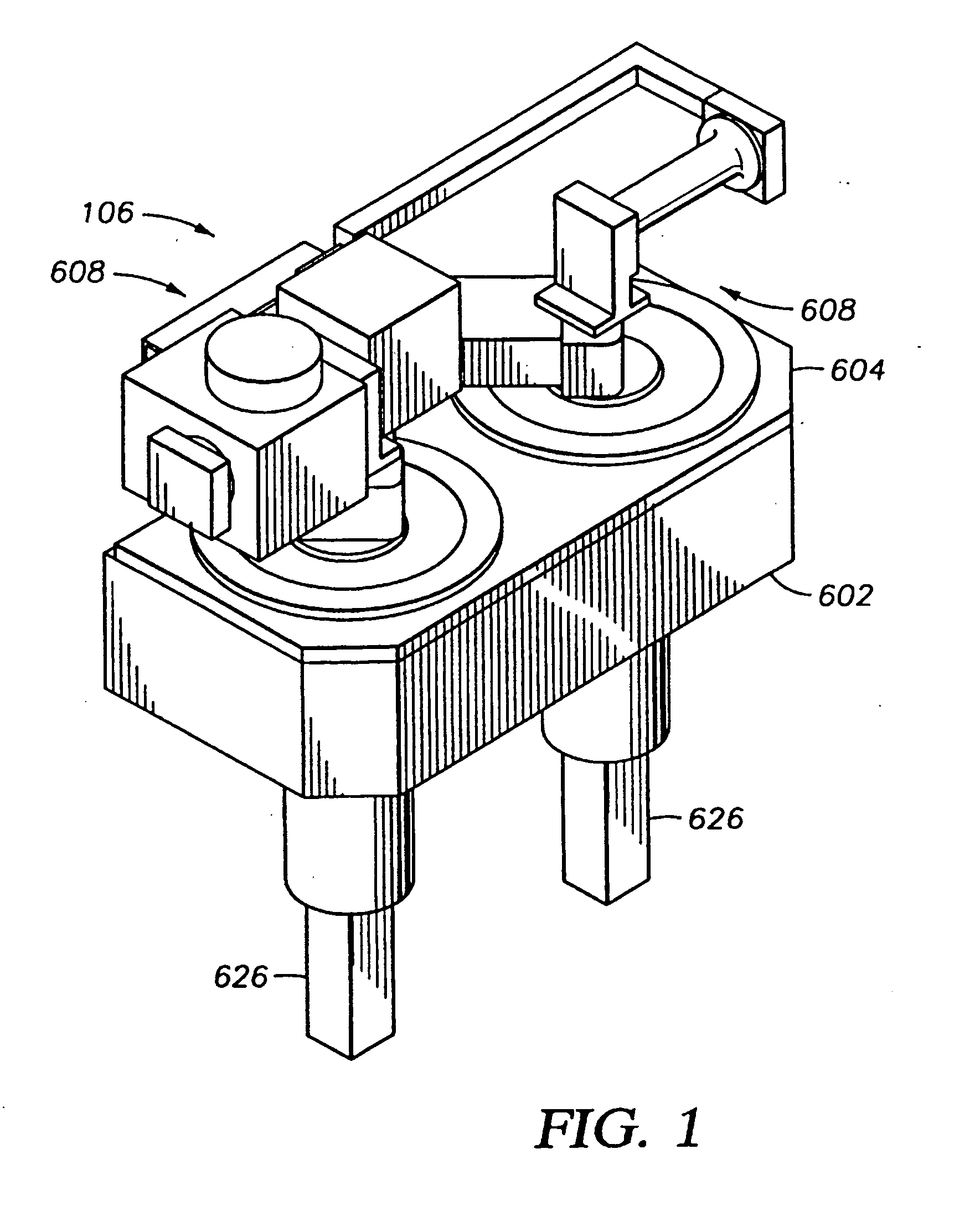
[0019]FIG. 1 shows a perspective view of one embodiment of a tandem processing chamber 106 of the present invention. Chamber body 602 is mounted or otherwise connected to a transfer chamber and includes two processing regions in which individual wafers are concurrently processed. The chamber body 602 supports a lid 604 which is hingedly attached to the chamber body 602 and includes one or more gas distribution systems 608 disposed therethrough for delivering reactant and cleaning gases into multiple processing regions.

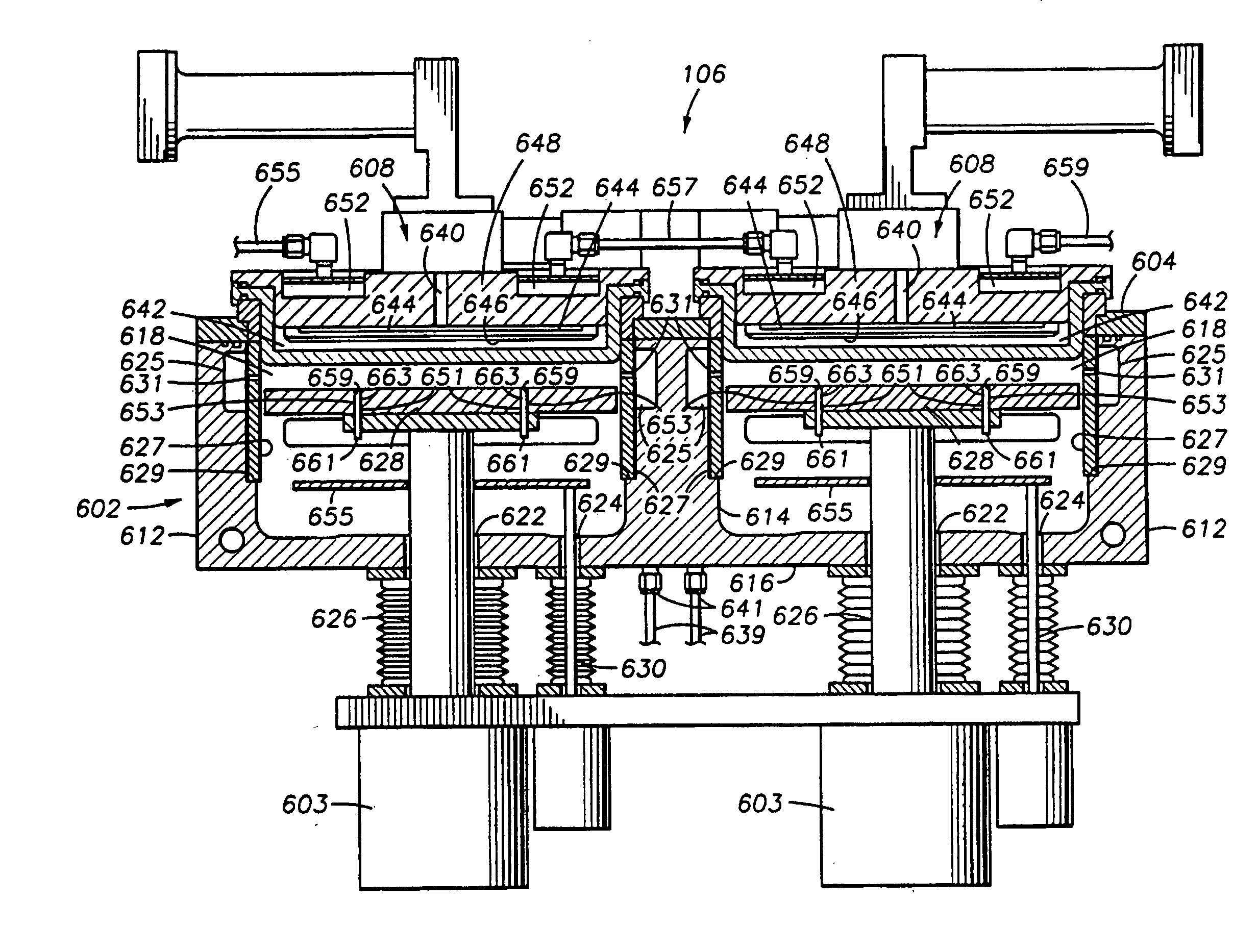
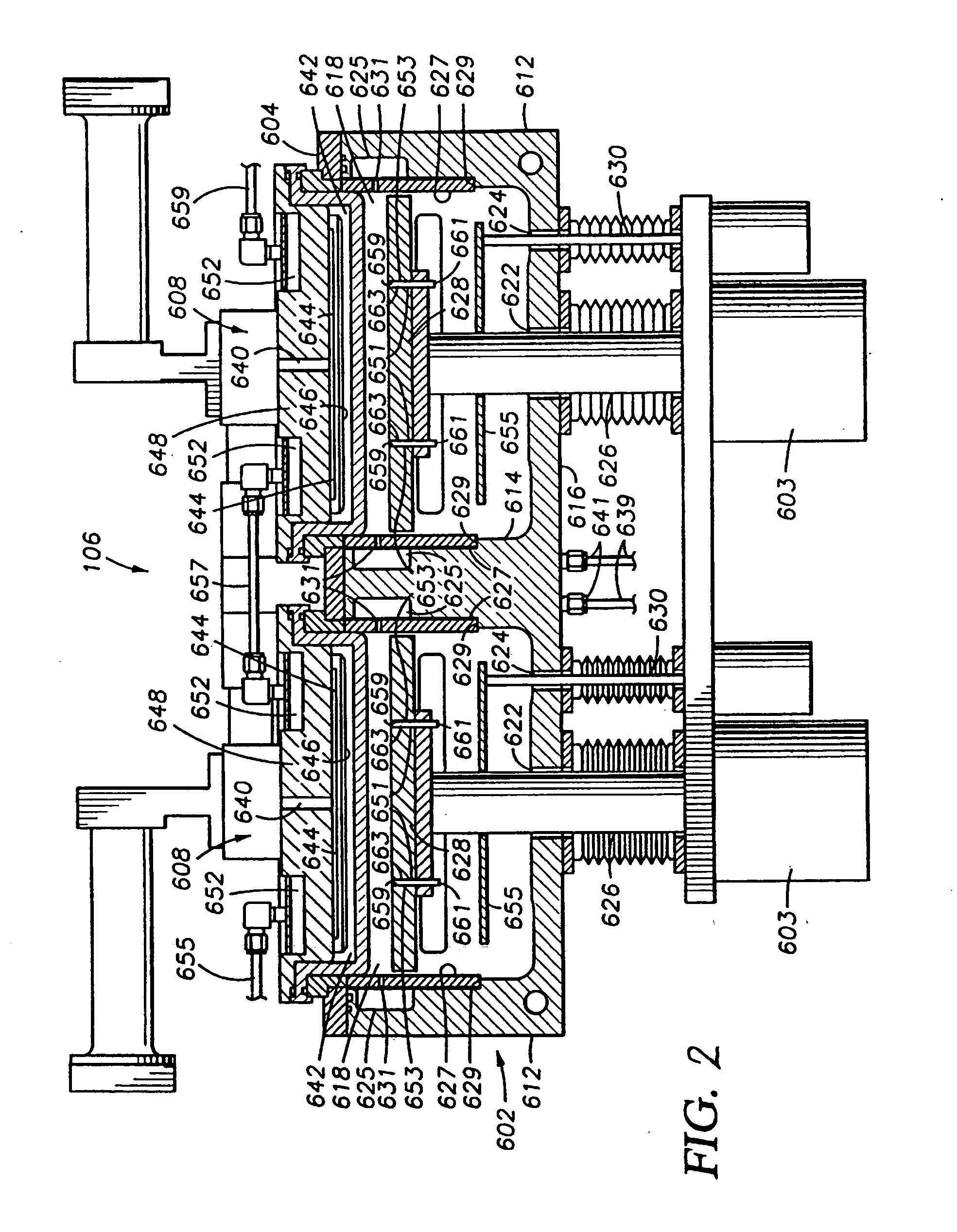
[0020]FIG. 2 shows a schematic cross-sectional view of the chamber 106 defining two processing regions 618, 620. Chamber body 602 includes sidewall 612, interior wall 614 and bottom wall 616 which define the two processing regions 618, 620. The bottom wall 616 in each processing region 618, 620 defines at least two passages 622, 624 through which a stem 626 of a pedestal heater 628 and a rod 630 of a wafer lift pin assembly are disposed, respectively. A pedestal lift ...


PUM

PropertyMeasurementUnit
temperatureaaaaaaaaaa
pressureaaaaaaaaaa
temperatureaaaaaaaaaa

Abstract

Embodiments of the present invention provide a method of reducing damage to the substrate support by the cleaning gas during a cleaning process of the processing chamber, such as by reducing aluminum fluoride formation on the substrate support. In one embodiment, a method of cleaning a semiconductor process chamber which is used for processing a substrate disposed on a surface of a substrate support comprises introducing a cleaning gas into a process chamber through an inlet facing a surface of a substrate support. The inlet is spaced from the surface of the substrate support by a clean spacing. Reactive species are provided from the cleaning gas to clean the process chamber. The clean spacing is substantially greater than a process spacing between the inlet and the surface of the substrate support during processing of a substrate on the substrate support in the process chamber.

Description

BACKGROUND OF THE INVENTION [0001] The present invention relates generally to semiconductor processing and, more particularly, to an improved process for cleaning a semiconductor processing chamber by minimizing negative effects of the cleaning procedure. [0002] One of the primary steps in the fabrication of modern semiconductor devices is the formation of a thin film on a semiconductor substrate by chemical reaction of gases. Such a deposition process is referred to as chemical vapor deposition (CVD). Conventional thermal CVD processes supply reactive gases to the substrate surface where heat-induced chemical reactions can take place to produce the desired film. Plasma enhanced CVD (PECVD) processes promote excitation and / or dissociation of reactant gases by application of radio frequency (RF) energy to the reaction zone proximate to the substrate surface thereby creating a plasma of highly reactive species. The high reactivity of the released species reduces the energy required fo...

Claims


Application Information

Patent Timeline
Patent Type & Authority Applications(United States)
IPC IPC(8): C25F3/12C23F1/00
CPCB08B7/0035C23C16/4405H01J37/32862H01J37/32477H01J37/32357
Inventor SUN, DAVIDHARVEY, KEITHINGLE, NITINJANAKIRAMAN, KARTHIK
Owner APPLIED MATERIALS INC
Learn More