
Dendrimer with triphenylamine core, organic memory device having the same, and manufacturing method thereof

a technology of dendrimer and organic memory, which is applied in the field of dendrimer, organic memory device and dendrimer manufacturing method, can solve the problems of increasing the manufacturing cost of memory chips, affecting the performance of memory devices, and difficulty in realizing high-capacity memory devices, etc., and achieves improved performance, improved integration, and reduced manufacturing cost.

Inactive Publication Date: 2012-07-10
SAMSUNG ELECTRONICS CO LTD
View PDF6 Cites 0 Cited by
  • Summary
  • Abstract
  • Description
  • Claims
  • Application Information

AI Technical Summary

Benefits of technology

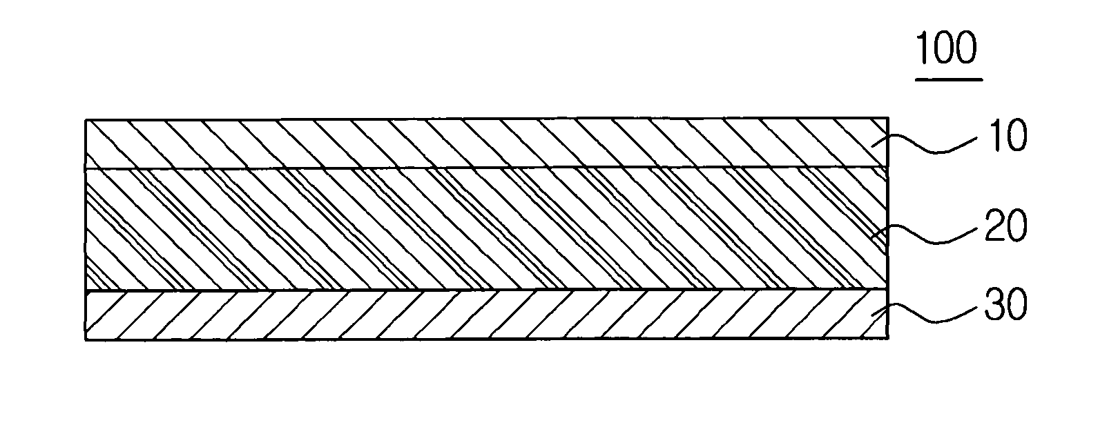
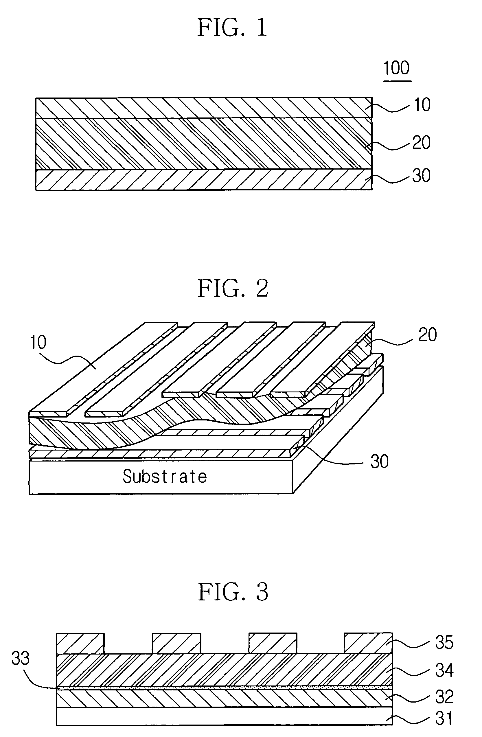
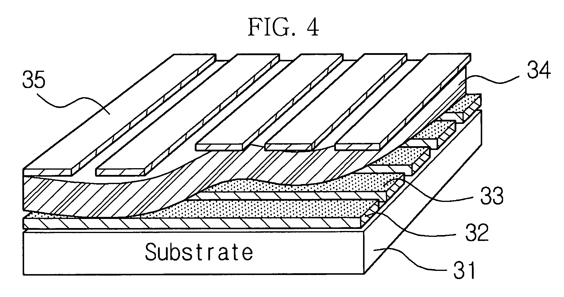
The patent describes a new type of molecule called a dendrimer, which has a triphenylamine core and a conjugated dendron without any heteroatoms. This dendrimer can be used in an organic memory device, which has lower manufacturing costs, higher integration, and faster switching compared to traditional memory devices. The patent also describes a method for manufacturing this organic memory device using a simpler process. Overall, the patent provides a new solution for creating efficient and cost-effective memory devices.

Problems solved by technology

However, these conventional memory devices may have a more complex structure and larger-sized memory cells.
Consequently, realizing higher capacity memory devices may be more difficult.
As a result, the manufacturing cost of memory chips may increase, and further miniaturization of the memory chips may be restricted by technical limitations, thus decreasing profitability.
However, when the semiconductor device is manufactured using the conductive polymer, realizing accurate molecular weight and distribution may be more difficult even if spin coating may be performed.
Thus, reproduction of the intermediate layer may not be easy, thereby resulting in less uniform device characteristics.
However, when a memory device is manufactured using fluorine polymer, a coating process may be more difficult to perform because of the hydrophobicity of fluorine, thereby decreasing processibility.
Furthermore, information may be recorded only once and must be read optically, thereby increasing the size and complexity of the device.

Method used


Image

  • Dendrimer with triphenylamine core, organic memory device having the same, and manufacturing method thereof
  • Dendrimer with triphenylamine core, organic memory device having the same, and manufacturing method thereof
  • Dendrimer with triphenylamine core, organic memory device having the same, and manufacturing method thereof

Examples


preparation example 1

Synthesis of 3STB-TAD

[0069]

[0070]As shown in Equation 1, 3,5-dibromo benzaldehyde and 4-tert-butyl styrene were stirred in dimethylacetamide (DMAC) together with sodium carbonate, 2,6-di-tert-butylcresol, and a palladium catalyst at a temperature of 130° C. for 48 hours. After the reaction was completed, the reaction mixture was diluted with methylene chloride (MC) and was then washed in water to separate an organic material layer. Then, the separated organic material layer was extracted therefrom, and was adsorbed on silica gel. Subsequently, dendron Stb-CHO was separated from the organic material layer, adsorbed on silica gel, through column chromatography, in which a subsidiary solvent having a volume ratio of hexane and methylene chloride of 2:1 (v / v) was used as a developing solvent.

[0071]To grow the synthesized dendron Stb-CHO by a generation, the Stb-CHO was put into a tetrahydrofuran (THF) solution together with methyltriphenylphosphonium iodide and potassium tert-butoxide a...

example 1

[0073]A glass substrate (Corning 1737) deposited with ITO was cut to a size of 0.5 mm×0.5 mm and patterned using photolithography and wet etching methods. The substrate was dipped into acetone and isopropyl alcohol, ultrasonically treated for 15 minutes, and dried. To form an organic active layer, 10 mg of the 3STB-TAD dendrimer obtained in Preparation Example 1 was put into 1 ml of chlorobenzene (C6H5Cl), and ultrasonically treated for 30 minutes, thus being dissolved to obtain a mixed solution. The mixed solution was passed through a syringe filter made of PTFE having 0.2 μm pores, and the glass substrate deposited with ITO was then spin-coated thereon with the mixed solution at a speed of 2000 rpm for 30 seconds. The coated substrate was baked on a hot plate at a temperature of 110° C. for 10 minutes, and thus the remaining solvent was removed therefrom. In this case, the thickness of the organic active layer was about 50˜100 nm, which was measured using an alpha-step profilomete...

experimental example

Switching Characteristics Test of Memory Device

[0074]The electrical characteristics of the memory device obtained in Example 1 were evaluated using a Keithley 4200 semiconductor characteristics analysis system. The switching characteristics of the memory device manufactured in Example 1 were evaluated depending variation in current and resistance by applying voltage to the memory device, and the results thereof are shown in FIG. 8.

[0075]Referring to FIG. 8, two conducting states are shown in the case where the memory device was swept in two + / − directions, based on a maximum voltage of 4V. When the memory device was swept by applying a negative bias voltage thereto, the characteristics of the memory device were changed into a low resistance state (SET state) at about −4 V, and a resistance state of 0 V was also maintained. In contrast, when the memory device was swept by applying a positive voltage thereto, the characteristics of the memory device were switched into a high resistanc...


PUM

PropertyMeasurementUnit
temperatureaaaaaaaaaa
volume ratioaaaaaaaaaa
sizeaaaaaaaaaa

Abstract

A dendrimer according to example embodiments may include a triphenylamine core, wherein a conjugated dendron having no heteroatoms is coupled to the triphenylamine core. An organic memory device according to example embodiments may include an organic active layer between a first electrode and a second electrode, wherein the organic active layer includes the dendrimer according to example embodiments. A barrier layer may be provided between the first and second electrodes. A method of manufacturing the organic memory device according to example embodiments may include forming an organic active layer between a first electrode and a second electrode, the organic active layer including the dendrimer according to example embodiments.

Description

PRIORITY STATEMENT[0001]This non-provisional application claims priority under 35 U.S.C. §119 to Korean Patent Application No. 10-2007-0032774, filed on Apr. 3, 2007 in the Korean Intellectual Property Office (KIPO), the entire contents of which are incorporated herein by reference.BACKGROUND[0002]1. Field[0003]Example embodiments relate to a dendrimer, an organic memory device having the dendrimer, and a method of manufacturing the organic memory device.[0004]2. Description of the Related Art[0005]The demand for memory devices has increased with the growth of information and communication industries. For example, the use of portable computers or electronic apparatuses (e.g., portable terminals, smart cards, electronic cash, personal digital assistants, digital audio players, and multimedia players) has increased. The memory devices for these apparatuses may be nonvolatile memory devices, wherein recorded information is not erased when power sources are turned off.[0006]As LSI (Larg...

Claims


Application Information

Patent Timeline
Patent Type & Authority Patents(United States)
IPC IPC(8): B32B15/04B32B9/04H01L51/00H10K99/00
CPCC07C211/54C08G61/12C08G83/003G11C13/0014G11C13/0016H01L51/0059H01L51/0095H01L51/0591C07C2103/18C08G2261/316C08G2261/3422G11C13/00H01L51/0038H01L51/0052H01L2251/308C07C2603/18Y10T428/31678H10K85/114H10K85/615H10K85/631H10K85/791H10K10/50H10K2102/103C08G61/00B82Y10/00
Inventor JOO, WON JAECHOI, TAE LIMKIM, CHULHEELEE, KWANG HEE
Owner SAMSUNG ELECTRONICS CO LTD
Learn More