Method of using group III-V ferromagnetic/non-magnetic semiconductor heterojunctions and magnetodiodes
a technology of non-magnetic semiconductors and ferromagnetic/non-magnetic semiconductors, applied in the direction of nanomagnetism, instruments, magnetic measurements, etc., can solve the problems of limiting the scalability of such devices, limiting the practical limitations of size reduction, and restricting the potential use and development of such devices, etc., to achieve linear increase in magnetoresistance, increase in magnetic field, increase in magnetoresistance
- Summary
- Abstract
- Description
- Claims
- Application Information
AI Technical Summary
Benefits of technology
Problems solved by technology
Method used
Image
Examples
example 1
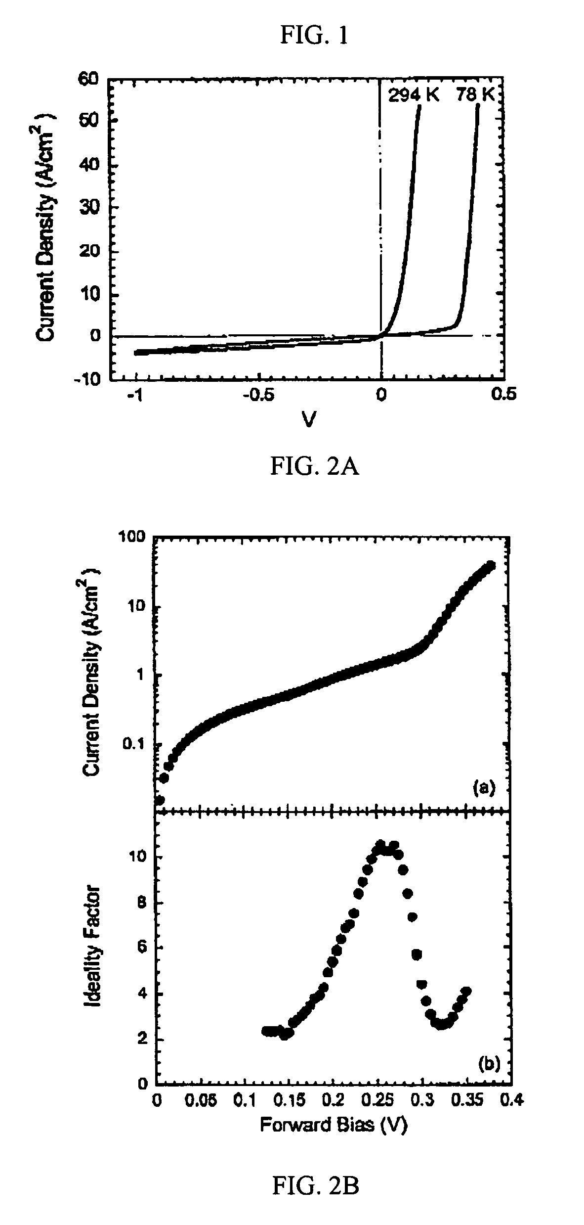
[0041]P-type In1-xMn,As films were deposited at 480° C. by atmospheric pressure metal-organic vapor phase epitaxy on nominally undoped, n-type InAs (100) substrates to form the heterojunctions. Precursors used were trimethylindium (TMIn), 0.3% arsine (AsH3) in hydrogen and tricarbonyl(methylcyclopentadienyl)manganese (TCMn). A pre-growth anneal at 510° C. was carried out under an arsine overpressure in order to remove surface oxide from the InAs substrate. A detailed description of the growth conditions for (In,Mn)As films has previously been reported. See, A. J. Blattner, J. Lensch, and B. W. Wessels, Journal of Electronic Materials 30, 1408 (2001). Manganese concentrations were determined using standards-based energy dispersive x-ray spectroscopy (EDS). X-ray diffraction was used to verify phase purity of the (In,Mn)As films. Film thickness, as determined by profilometry, ranged from about 100—about 525 nm. Room temperature hole concentrations of (In,Mn)As films are on the order o...
example 2
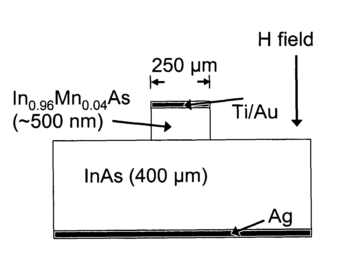
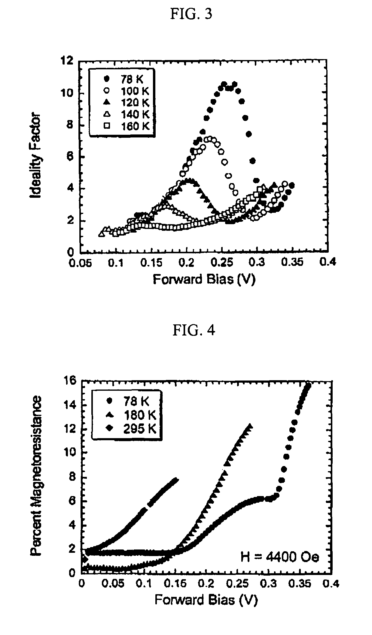
[0042]Mesa diodes were fabricated from the epitaxial structures using conventional photolithography and a citric acid wet etch. See, G. C. Desalvo, R. Kaspi, and C. A. Bozada, J. Electrochem. Soc. 141, 3526 (1994). The mesa diameter was 250 μm. Ti / Au (15 / 175 nm) ohmic contacts were evaporated to the (In,Mn)As films. Silver paste was used to make contact to the InAs substrates. The diodes were wire bonded to a non-magnetic chip carrier with gold wire. Low-temperature measurements were carried out in a Janis ST-100 cryostat with a non-magnetic sample holder. A Keithley 2400 source-meter was used to source voltages and measure currents. Magnetoresistance measurements were made in fields of up to 4600 Oe applied parallel to current flow across the junction.
[0043]Using a similar approach, high field, longitudinal magnetoresistance measurements were taken on a p-In0.96Mn0.04As / n-InAs junction. A nonsaturating linear magnetoresistance at fields greater than 1.5 T was observed at room tempe...
example 3
[0044]For these studies, a 500 nm thick p-In0.96Mn0.04As layer was deposited on an undoped n-InAs substrate using atmospheric pressure metal-organic vapor phase epitaxy under conditions previously described. (A. J. Blattner, J. Lensch, and B. W. Wessels, J. Electron. Mater. 30, 1408 (2001).) The room temperature electron concentration of the InAs substrate is 2×1016 cm−3, while the room temperature hole concentration of the p-InMnAs film is on the order of 1018-1019 cm−3. The diodes were patterned into 250 μm diameter mesas using photolithography and wet etching Ti / Au was used as the p-In0.96Mn0.04As ohmic contact, while Ag was used as the n-InAs ohmic contact. Magnetoresistance measurements were made with the magnetic field applied parallel to the flow of current through the mesa diode using a Quantum Design Physical Properties Measurement System. A schematic of the experimental setup is shown in FIG. 7.
PUM
 Abstract
Description
Claims
Application Information
 - R&D
- Intellectual Property
- Life Sciences
- Materials
- Tech Scout
- Unparalleled Data Quality
- Higher Quality Content
- 60% Fewer Hallucinations
Browse by: Latest US Patents, China's latest patents, Technical Efficacy Thesaurus, Application Domain, Technology Topic, Popular Technical Reports.
© 2025 PatSnap. All rights reserved.Legal|Privacy policy|Modern Slavery Act Transparency Statement|Sitemap|About US| Contact US: help@patsnap.com


