Manufacturing method of semiconductor substrate

a manufacturing method and semiconductor technology, applied in the direction of semiconductor devices, basic electric elements, electrical apparatus, etc., can solve the problems of easy generation of defect levels, low efficiency of semiconductor elements manufactured using this single crystal semiconductor layer, and increase defects in single crystal semiconductor layers. , to achieve the effect of improving efficiency in manufacturing a semiconductor substra

Inactive Publication Date: 2011-03-22
SEMICON ENERGY LAB CO LTD
View PDF55 Cites 1 Cited by
  • Summary
  • Abstract
  • Description
  • Claims
  • Application Information

AI Technical Summary

Benefits of technology

[0010]As an alternative method, a method for irradiating a single crystal semiconductor layer with a laser beam is given, for example. By irradiation with a laser beam, only the single crystal semiconductor layer is selectively melted, whereby defects can be reduced. As the laser beam, a pulse-oscillation laser beam is mainly used. The pulse-oscillation laser beam (hereinafter also referred to as a pulsed laser beam) has an advantage that a desired intensity is easily obtained as compared to the case of using a continuous-wave laser beam (hereinafter also referred to as a CW laser beam).
[0011]Here, in the case of irradiating a single crystal semiconductor layer with a pulsed laser beam, there is a problem in that surface unevenness of the single crystal semiconductor layer increases in a region irradiated with an edge portion of a pulsed laser beam. This is caused because a melted region and an unmelted region are mixed in the irradiated region and, therefore, a distortion is easily generated at a boundary between the melted region and the unmelted region in the single crystal semiconductor layer. As a method of reducing such a distortion, a method in which irradiation with many pulsed laser beams is performed while the irradiation position is moved little by little can be given; however, this method has a problem of low throughput.
[0012]In consideration of the above-described problems, it is an object to improve planarity of a surface of a semiconductor layer in a semiconductor substrate. Further, it is another object to improve productivity of semiconductor substrates.
[0021]In the invention disclosed in this specification, a laser beam is shaped in accordance with the shape or the like of an island-shaped semiconductor layer. Alternatively, a semiconductor layer is patterned in accordance with an irradiation region of a laser beam. Accordingly, a semiconductor layer is not irradiated with an edge portion of a laser beam but is irradiated with a center portion of a laser beam, whereby surface unevenness caused by irradiation with the edge portion of the laser beam can be suppressed and a semiconductor substrate including a highly planar semiconductor layer can be provided. In addition, since irradiation with many pulsed laser beams for suppressing the surface unevenness is not needed, efficiency in manufacturing a semiconductor substrate can be improved.

Problems solved by technology

In the case where a single crystal semiconductor layer is formed by using an ion-implantation separation method in the above-described manner, the ion implantation increases defects in the single crystal semiconductor layer.
In a situation that many defects exist in a single crystal semiconductor layer, defect levels are easily generated at the interface with a gate insulating film, for example; accordingly, a semiconductor element manufactured using this single crystal semiconductor layer does not have favorable characteristics.
Further, in the case where many defects exist in a single crystal semiconductor layer, original characteristics of the single crystal semiconductor cannot be obtained.
However, heating at a high temperature or treatment such as grinding and polishing is not appropriate for treatment on a single crystal semiconductor layer formed over a glass substrate.
Here, in the case of irradiating a single crystal semiconductor layer with a pulsed laser beam, there is a problem in that surface unevenness of the single crystal semiconductor layer increases in a region irradiated with an edge portion of a pulsed laser beam.
This is caused because a melted region and an unmelted region are mixed in the irradiated region and, therefore, a distortion is easily generated at a boundary between the melted region and the unmelted region in the single crystal semiconductor layer.
As a method of reducing such a distortion, a method in which irradiation with many pulsed laser beams is performed while the irradiation position is moved little by little can be given; however, this method has a problem of low throughput.

Method used


Image

  • Manufacturing method of semiconductor substrate
  • Manufacturing method of semiconductor substrate
  • Manufacturing method of semiconductor substrate

Examples


embodiment mode 1

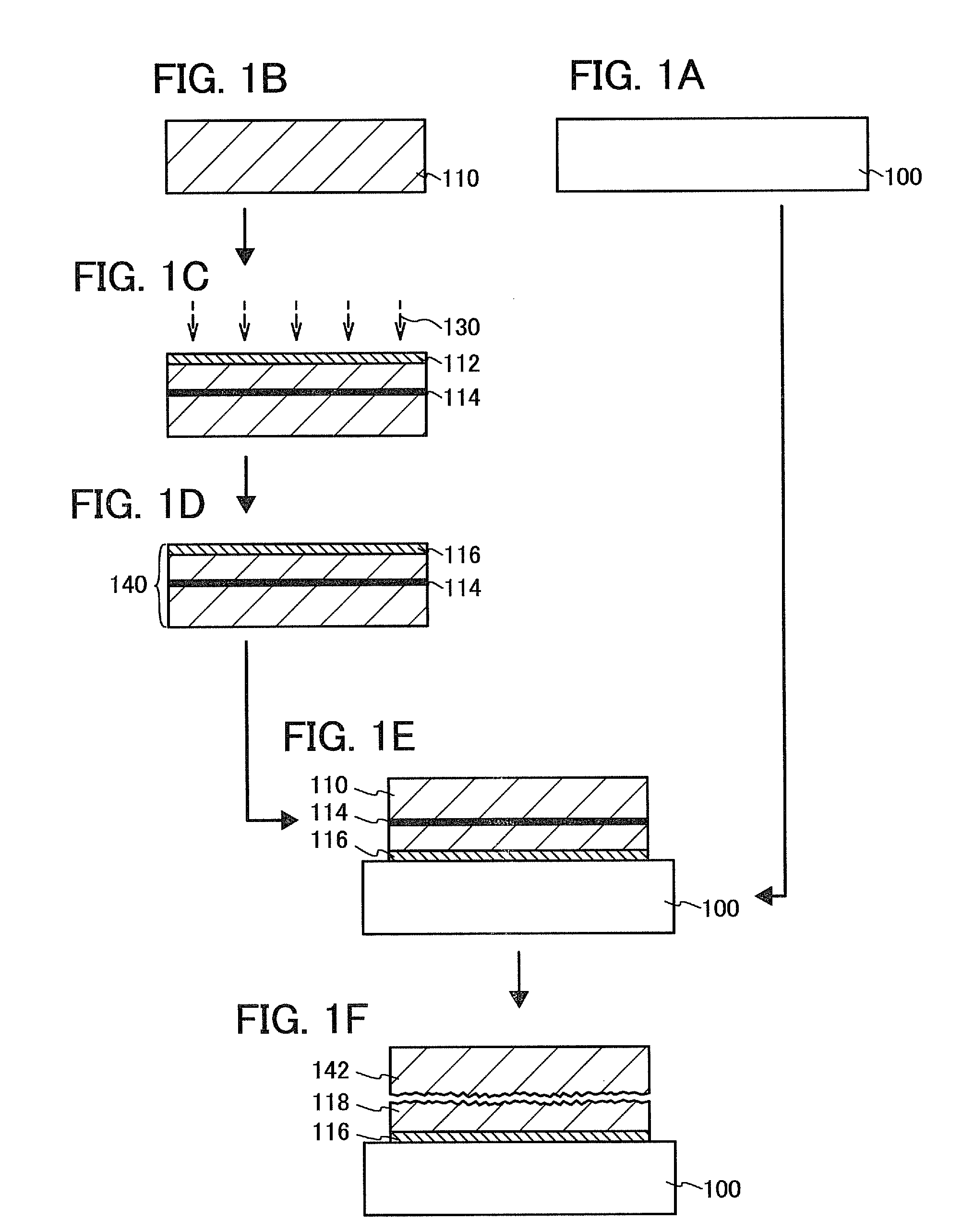
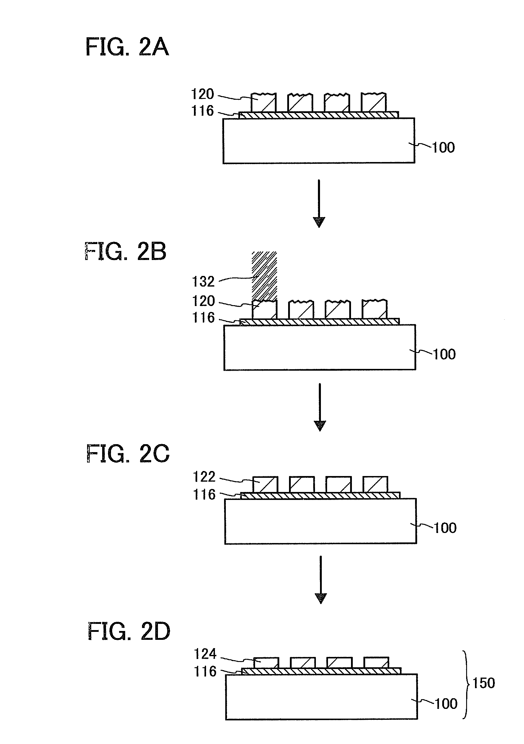
[0041]In Embodiment Mode 1, a manufacturing method of a semiconductor substrate will be described with reference to FIGS. 1A to 1F, FIGS. 2A to 2D, FIGS. 3A to 3C, and FIGS. 4A to 4C.

[0042]First, a base substrate 100 is prepared (see FIG. 1A). As the base substrate 100, a visible light transmitting glass substrate used for a liquid crystal display device or the like can be used, for example. As a glass substrate, a substrate having a strain point of equal to or higher than 580° C. and equal to or lower than 680° C. (preferably, equal to or higher than 600° C. and equal to or lower than 680° C.) may be used. Further, it is preferable that the glass substrate be a non-alkali glass substrate. As a material of the non-alkali glass substrate, a glass material such as aluminosilicate glass, aluminoborosilicate glass, or barium borosilicate glass is used, for example.

[0043]Note that as the base substrate 100, as well as the glass substrate, an insulating substrate which is formed of an ins...

embodiment mode 2

[0096]In Embodiment Mode 2, the relationship between the island-shaped semiconductor layers and the irradiation regions of pulsed laser beams in the manufacturing method of a semiconductor substrate described in Embodiment Mode 1 will be described with reference to FIGS. 5A and 5B. FIGS. 5A and 5B each illustrate a mode where rectangular semiconductor layers and rectangular pulsed laser beams (planar pulsed laser beams) are used; however, the invention disclosed in this specification is not limited to this.

[0097]FIG. 5A illustrates a mode where one island-shaped semiconductor layer 502 formed over a base substrate500 is irradiated with one pulsed laser beam. Here, the irradiation region of the pulsed laser beam is shown by a region 504 (the region shown by a broken line in FIG. 5A). Note that the irradiation region of the pulsed laser beam means a region irradiated with a pulsed laser beam having an intensity equal to or higher than the threshold value Ith in Embodiment Mode 1. Here...

embodiment mode 3

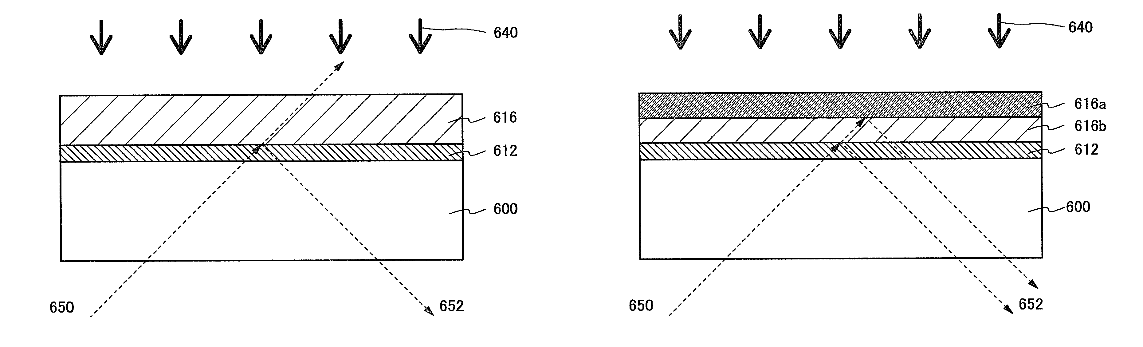
[0102]In Embodiment Mode 3, an evaluation method which can be used for a manufacturing method of a semiconductor substrate will be described with reference to FIGS. 6A and 6B, FIGS. 7A and 7B, FIGS. 8A and 8B, and FIGS. 9A and 9B. First, an evaluation method of a semiconductor layer utilizing change in reflectance of a reference beam, with which a semiconductor layer is irradiated, depending on the melted state of the semiconductor layer and this nature, will be described with reference to FIGS. 6A and 6B and FIGS. 7A and 7B. In description with reference to FIGS. 6A and 6B and FIGS. 7A and 7B, the case where only the irradiation intensity of a pulsed laser beam is changed with a fixed irradiation time (pulse width) and a fixed irradiation pulse number will be described for simplicity.

[0103]In FIGS. 6A and 6B, a semiconductor layer 616 is formed over an insulating layer 612 and the insulating layer 612 is formed over a base substrate 600. Note that the semiconductor layer 616 is irr...


PUM


Abstract

A surface of a single crystal semiconductor substrate is irradiated with ions to form a damaged region, an insulating layer is formed over the surface of the single crystal semiconductor substrate, and a surface of a substrate having an insulating surface is made to be in contact with a surface of the insulating layer to bond the substrate having an insulating surface to the single crystal semiconductor substrate. Then, the single crystal semiconductor substrate is separated at the damaged region by performing heat treatment to form a single crystal semiconductor layer over the substrate having an insulating surface, and the single crystal semiconductor layer is patterned to form a plurality of island-shaped semiconductor layers. One of the island-shaped semiconductor layers is irradiated with a laser beam which is shaped to entirely cover the island-shaped semiconductor layer.

Description

BACKGROUND OF THE INVENTION[0001]1. Field of the Invention[0002]The present invention relates to a manufacturing method of a semiconductor substrate.[0003]2. Description of the Related Art[0004]In recent years, integrated circuits using an SOI (silicon on insulator) substrate, instead of using a bulk silicon substrate, have been developed. By utilizing the characteristics of a thin single crystal silicon layer formed over an insulating layer, transistors formed in the integrated circuit can be completely separated from each other, and further, the fully depleted transistors can be formed. Accordingly, a semiconductor integrated circuit with high added value such as high integration, high speed driving, and low power consumption can be realized.[0005]As a manufacturing method of an SOI substrate, a hydrogen-ion-implantation separation method in which hydrogen ion implantation and separation are combined is known. A typical process of the hydrogen-ion-implantation separation method wi...

Claims


Application Information

Patent Timeline
Patent Type & Authority Patents(United States)
IPC IPC(8): H01L21/20H01L21/36
CPCH01L21/76254H01L21/84H01L29/78621H01L29/66772H01L29/458
Inventor TANAKA, KOICHIRO
Owner SEMICON ENERGY LAB CO LTD
Why Eureka
Try Eureka