Image forming apparatus and image forming process

Inactive Publication Date: 2010-05-11
RICOH KK
View PDF25 Cites 1 Cited by
  • Summary
  • Abstract
  • Description
  • Claims
  • Application Information

AI Technical Summary

Benefits of technology

[0023]As to the former, by irradiating a photoconductor with light, a charge-eliminating unit functions to decay a residual potential on the photoconductor, reduce a potential difference between an exposed portion using a writing light and an unexposed portion and uniform a photoconductor surface potential for the next time the photoconductor surface is charged.
[0024]When the linear velocity of a photoconductor is constant, and a margin of photoconductor potential decay is small because of charge elimination (for example, light intensity is small, the responsiveness of a photoconductor is poor, and sensitivity is small), it is necessary to shift an arrangement of a charge-eliminating member in a direction which is advantageous in an image forming process. Assuming that there is a margin in charging ability, it is possible to reduce a charging member in size and to enlarge the space between a charge-eliminating unit and a charging unit. Thus, it is possible to lengthen a charge-eliminating light irradiation time and to lengthen a time after charge-eliminating light irradiation. Specifically, it becomes possible to provide a time space for decaying a residual potential on a photoconductor and uniforming the surface potential of the photoconductor.
[0047]Thus, (1) since the photoconductor surface potential does not lower sufficiently, it is impossible to obtain developing potential sufficiently, which causes such a trouble that the image density decreases in negative-positive developing; (2) even if developing potential can be gained, the surface potential decrease still continues when the exposed site is past the developing site, and toner is developed at an exposed portion in negative-positive developing (attachment of toner is conducted electrostatically); thus, the adhesion between the exposed portion and the toner lowers, and an increase in the resolution of dots or dust at the time of transfer is liable to arise; (3) further, when the photoconductor has rotated once passing image forming elements and then enters a next step, carriers later generated inside at a next time of charging cause the potential of a former image exposed portion to decrease slightly. Accordingly, there is a difference in halftone potential, which causes abnormal images like ghosts (afterimages) to arise in monochrome machines, and which causes color reproducibility to lower in the case of full-color machines which produce a lot of halftone images.
[0069]As is evident from the detailed and specific explanations below, the present invention makes it possible to provide a compact image forming apparatus capable of solving various problems in related art and forming high-quality images at high speed, and an image forming process using the image forming apparatus; also, the present invention makes it possible to provide an image forming apparatus which is high in durability and capable of stable image output with few abnormal images, even when repeatedly used, and an image forming process using the image forming apparatus, hence a very superior effect.
[0070]The present inventors have worked out a rate-limiting process in an image forming process allowing for obtaining the compactness, high-speed performance (50 sheets / min or more) and high resolution (1,200 dpi or more). As a result of it, some facts are revealed. To achieve high-speed performance with maintaining a small diameter of a photoconductor, it is necessary to increase the linear velocity of the photoconductor, but the required linear velocity varies according to the set printing speed and the paper gap. When a target printing speed is constant, the smaller the paper gap is, the smaller the photoconductor linear velocity can be set; however, the paper gap has a lower limit, and the photoconductor linear velocity is naturally set with its lower limit.
[0105]According to the present invention, it is possible to provide a compact image forming apparatus capable of solving various problems in related art and forming high-quality images at high speed, and an image forming process using the image forming apparatus. Also, it is possible to provide an image forming apparatus which is high in durability and capable of stable image output with few abnormal images, even when repeatedly used, and an image forming process using the image forming apparatus.

Problems solved by technology

In recent years, image forming apparatuses allowing for achievement of high image quality of 1,200 dpi or more have had two major problems to solve.
An image forming apparatus based upon a “tandem system”, which is the former, produces a large number of printed sheets per unit time but has problems with a large size of the apparatus and its high costs because image-forming processors such as a charger and a laser scanner unit are necessary for each image forming unit; whereas, an image forming apparatus based upon a “one-drum system”, which is the latter, makes it not necessary to improve positional accuracy as high as that of the “tandem system” because displacement of an output image caused by using a plurality of photoconductor drums is vanishingly small in comparison with the “tandem system”, thereby making it possible to reduce costs caused by using four photoconductor drums.
However, in the “one-drum method”, there is a problem that it takes approximately four times longer for the “one-drum system” to form a full-color image by means of four colors of yellow, magenta, cyan and black than to obtain a monochrome image of black color, and thus the productivity in producing full-color images per unit time (printing speed) is low.
However, in conventional image forming apparatuses, since members constituting image forming elements such as for a charging step and a writing step are slow in ability, it has been difficult to plan compactness, high-speed performance (50 sheets / min or more) and high resolution (1,200 dpi or more).
It is not impossible for a wire-type charging member used thus far, which is typified by a scorotron charger, to increase the amount of a corona falling onto the surface of the photoconductor by increasing the number of wires, but there is a problem that when wires are too close to one another in distance, they interfere with one another and power consumption becomes greater.
For this reason, when the diameter of a photoconductor is lessened, a grid-photoconductor surface distance significantly differs between the center and both ends of a grid, and the net nip width becomes very small (charging becomes unstable at both ends that are front and rear ends corresponding to the moving direction of the photoconductor).
However, an apparatus has to be a little complex to place such a photoconductor in, and the space in which a charging member can be placed is inevitably small due to the reduction in diameter; thus, this method is not realistic.
However, owing to the AC superimposition to obtain greater charging ability, there is a greater hazard to the photoconductor surface, and so the impact on the durability (lifetime) of the photoconductor will be great.
Therefore, at this point in time, an LED is hardly deemed to be most suitable as a light source of 1200 dpi or more.
However, at present the number of rotations of a polygon mirror is 40,000 rpm or so at the most, and a single beam causes a limit on writing speed.
Meanwhile, in actual fact, as to related art such as the one described above, when compactness and high-speed performance are to be realized at the same time, it is not much clear where a rate-limiting factor is, in process designing, owing to the relationships between the linear velocity of a photoconductor, the size of members disposed in the vicinity of the photoconductor, and their respective abilities; furthermore, photoconductor techniques to respond to demands for compactness and high-speed performance have yet to become clear.

Method used


Image

  • Image forming apparatus and image forming process
  • Image forming apparatus and image forming process
  • Image forming apparatus and image forming process

Examples


embodiments

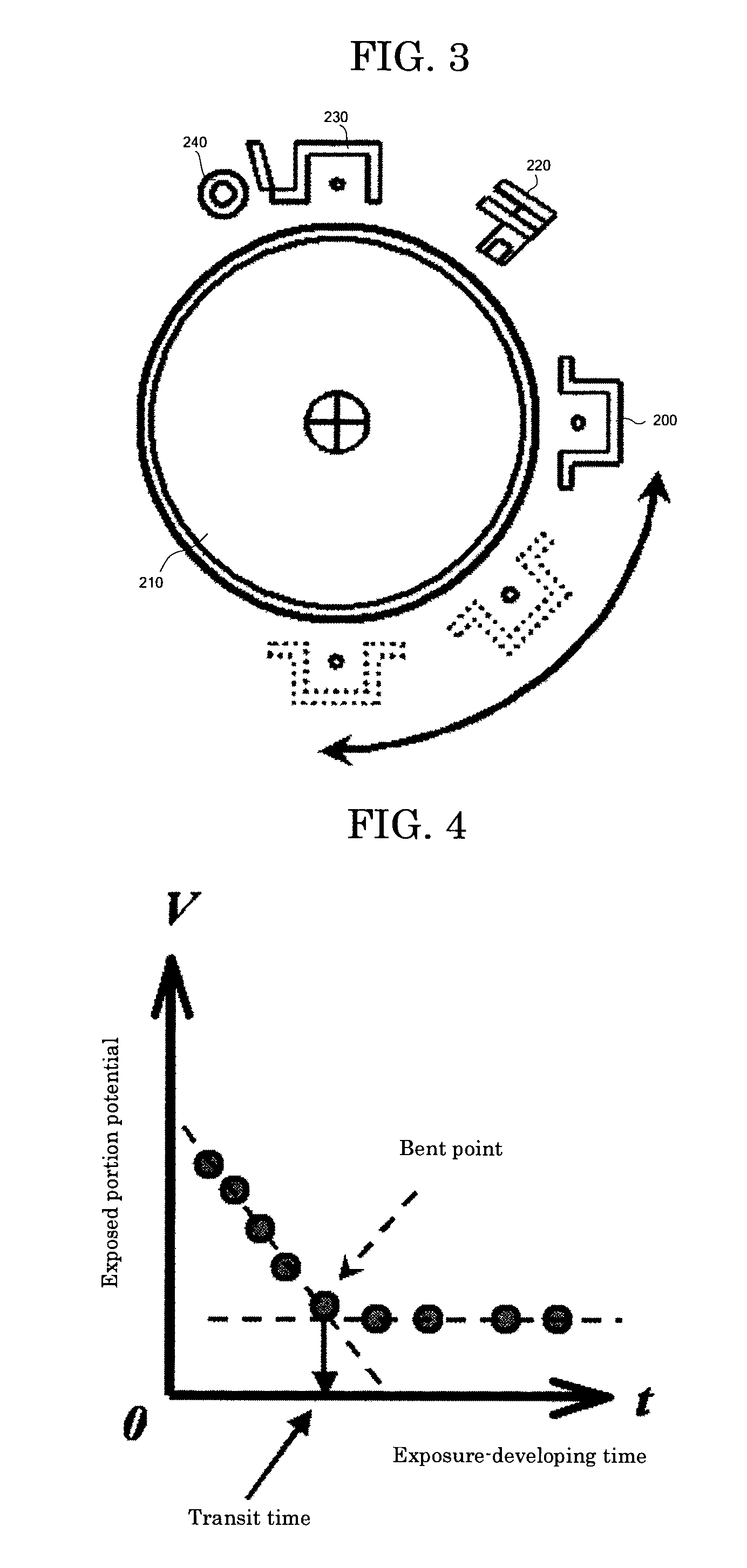
[0211]In FIG. 16, one example of an image forming apparatus of the present invention is shown as Embodiment B-1. The image forming apparatus in FIG. 16 is a full-color image forming apparatus (of four colors) according to an electrophotographic system, and the figure is a longitudinally cross-sectional view schematically showing the schematic structure thereof. Examples of the image forming apparatus include a printer, a copier and a facsimile.

[0212]The image forming apparatus in the figure is provided with a color image forming unit which forms color images (images of colors except black), and a black image forming unit which forms black images, including drum-shaped electrophotographic photoconductors (hereinafter referred to as “photoconductors”) (301) and (310) respectively. Amongst these photoconductors, the photoconductor (301) (first photoconductor) is for forming color images, and the photoconductor (310) (second photoconductor) is for forming black images. Note that hereina...

examples

[0427]Hereinafter, the present invention will be further described referring to specific Examples, however, the present invention is not limited to the following Examples. Note that the following unit term of “part” or “parts” respectively means “part by mass” or “parts by mass”.

[0428]First, the method of synthesizing an azo pigment and a titanylphthalocyanine crystal will be described. The azo pigments used in the following Examples were prepared according to the method described in Japanese Patent Application Laid-Open (JP-A) No. 60-29109 and Japanese Patent (JP-B) No. 3026645. The titanylphthalocyanine crystal used in the following Examples was prepared according to the method described in Japanese Patent (JP-B) No. 2004-83859.

—Synthesis of Titanylphthalocyanine Crystal

synthesis example a-1

[0429]A pigment was produced according to the Example 1 described in Japanese Patent Application Laid-Open (JP-A) No. 2004-83859.

[0430]Specifically, 292 g of 1,3-diiminoisoindline and 1,800 parts of sulfolane were mixed, and 20.4 g of titanium tetrabutoxide was delivered by drops into the mixture in a nitrogen gas stream. Upon completion of the dropping, the temperature of the mixture was gradually increased to 180° C. and then stirred and reacted for 5 hours while keeping the reaction temperature from 170° C. to 180° C. After completion of the reaction, the reactant was naturally cooled, and the precipitate was filtered and the filtrated precipitate was washed until the powder of the precipitate turned into blue by chloroform. Next, the powder was washed with methanol several times and further washed with 80° C. hot water several times and then dried to obtain a coarse titanylphthalocyanine. The coarse titanylphthalocyanine was dissolved in 20 times its volume of a sulfuric acid, a...


PUM


Abstract

The present invention provides an image forming apparatus including a photoconductor, a charging unit configured to charge the photoconductor, a writing unit configured to form a latent electrostatic image, a toner image forming unit configured to form a toner image by developing the latent electrostatic image, the toner image forming unit having a plurality of developing devices housing a plurality of color developers for each color, a transfer unit configured to transfer the toner image formed on the photoconductor onto a transfer material, and a fixing unit configured to fix the transferred toner image on the transfer material, wherein the time spent by an arbitrary point on the photoconductor in moving from a position in which to face the writing unit to a position in which to face the developing unit is shorter than 50 ms and longer than the transit time of the photoconductor.

Description

BACKGROUND OF THE INVENTION[0001]1. Field of the Invention[0002]The present invention relates to an image forming apparatus which is compact and operates at high speed, and an image forming process.[0003]2. Description of the Related Art[0004]In recent years, image forming apparatuses allowing for achievement of high image quality of 1,200 dpi or more have had two major problems to solve. One is a demand for achievement of high-speed performance, and the other is a demand for achievement of compactness.[0005]For the former, in order to improve productivity in image forming apparatuses, improvement in printing speed is vital. As for a monochrome machine, measures are generally taken by increasing the linear velocity of a photoconductor (hereinafter possibly referred to as “electrophotographic photoconductor”, “latent electrostatic image-bearing member”, “image-bearing member” or “photoconductive insulator”) and enlarging the diameter of the photoconductor. As for a full-color machine...

Claims


Application Information

Patent Timeline
IPC IPC(8): B41J2/45G03G5/05G03G5/07
CPCG03G15/751G03G15/011
Inventor INABA, YOSHINORINIIMI, TATSUYA
Owner RICOH KK
Why Eureka
Try Eureka