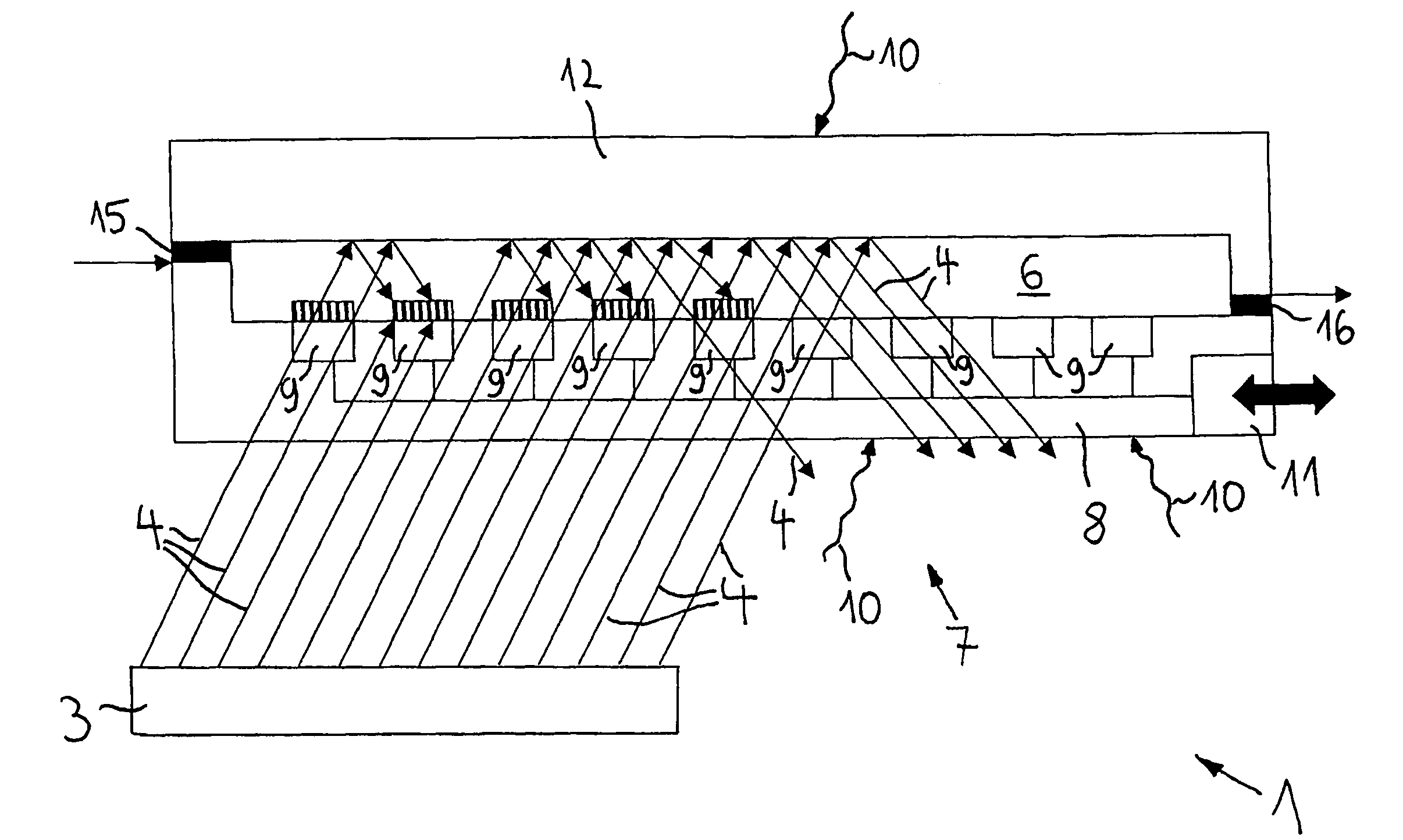
[0009]The
semiconductor substrate thereby advantageously performs a
dual function, and in addition to acting as the support for the at least one radiation receiver, also acts as a window for the injection of the excitation radiation into the measurement chamber. The measurement chamber can then be manufactured particularly economically using Microsystems
engineering methods. The device can thereby have very compact dimensions. The measurement chamber shields, in the
wavelength range that can be detected with the radiation receiver, the at least one radiation receiver that is located in the measurement chamber or within its external contour against scattered or spurious radiation that occurs outside the measurement chamber. Any spurious radiation that penetrates into the wall of the measurement chamber is thereby either completely extinguished or is at least so severely attenuated that after it penetrates the wall it is practically no longer detected by the radiation receiver. Thus, in the
wavelength range to be detected, the measurement has a high level of protection against interference from scattered or spurious radiation.
[0013]In one preferred embodiment of the invention, the luminescent substance is realized so that the
wavelength of the luminescent radiation is less than the
excitation wavelength. Upward-converting luminescent substances of this type are described in the prior art, such as EP 0 723 146 A1, for example. Examples of upward-converting luminescent substances are the BND
pigment manufactured by Dyomics GmbH, Jena and IR-140. In contrast to downward-converting luminescent substances, upward-converting luminescent substances acquire the energy necessary for the
quantum emission not from a single
quantum effect, but from a plurality of
quantum effects. Upward-converting luminescent substances therefore have, in comparison to downward-converting luminescent substances, a significantly greater
Stokes shift, at which the wavelength of the excitation radiation can be, for example, twice as great as the wavelength of the luminescent radiation. Consequently it is possible to provide, as the radiation source, an
infrared semiconductor radiation source, in particular a
semiconductor diode, which makes it possible to have a
high radiation intensity with compact dimensions. The
infrared light from such semiconductor radiation sources also has the
advantage that fewer spurious effects occur than with short-wave
optical radiation. By means of the upward-converting luminescent substance, the
optical radiation emitted by the semiconductor radiation source can be converted into visible light or into near-
infrared light, so that an economical opto-electronic
semiconductor sensor can be provided as the radiation receiver, which has a high detection sensitivity in this
wavelength range.
[0014]It is advantageous if a boundary wall of the measurement chamber that is opposite the wall area is realized in the form of a reflector for the reflection of the excitation radiation. The radiation injected into the measurement chamber can then be used more efficiently for the excitation of the at least one luminescent substance.
[0019]In one preferred embodiment of the invention, in the interior cavity, at least one
receptor for a ligand, in particular for a
biomolecule, a
biological cell and / or at least one fragment thereof is immobilized on the surface of at least one radiation receiver, whereby the ligand is marked with the at least one luminescent substance. In this case, the term “
receptor” means a molecule that can be bonded to a surface and can enter into a bond with a second molecule, the ligand. Receptors include, for example, but are not limited to: nucleic acids and derivatives thereof (
DNA,
RNA, PNA, LNA, oligonucleotides, plasmids,
chromosome), peptides and proteins (enzymes, proteins, oligopeptides,
cellular receptor proteins and complexes thereof,
peptide hormones, antibodies and fragments thereof), carbohydrates and byproducts thereof, in particular glycolized proteins and glycosides. The
receptor, however, can also include more complex structures such as cells and fragments thereof, for example. The term “ligands” as used here means molecules that can form a more or less specific bond with a receptor. Ligands include, for example, but are not limited to: nucleic acids and derivatives thereof (
DNA,
RNA, PNA, LNA, oligonucleotides, plasmids, chromosomes), peptides and proteins (enzymes, proteins, oligopeptides,
cellular receptor proteins and complexes thereof,
peptide hormones, antibodies and fragments thereof, carbohydrates and derivatives thereof, in particular glycolized proteins and glycosides, gats, fatty acids and lipids, cells and fragments thereof, as well as all pharmacologically and toxicologically active substances. The receptor can be imprinted on the radiation receiver, if necessary. A
polyimide layer can be placed between the radiation receiver and the receiver to improve the adherence of the receptor to the radiation receiver.
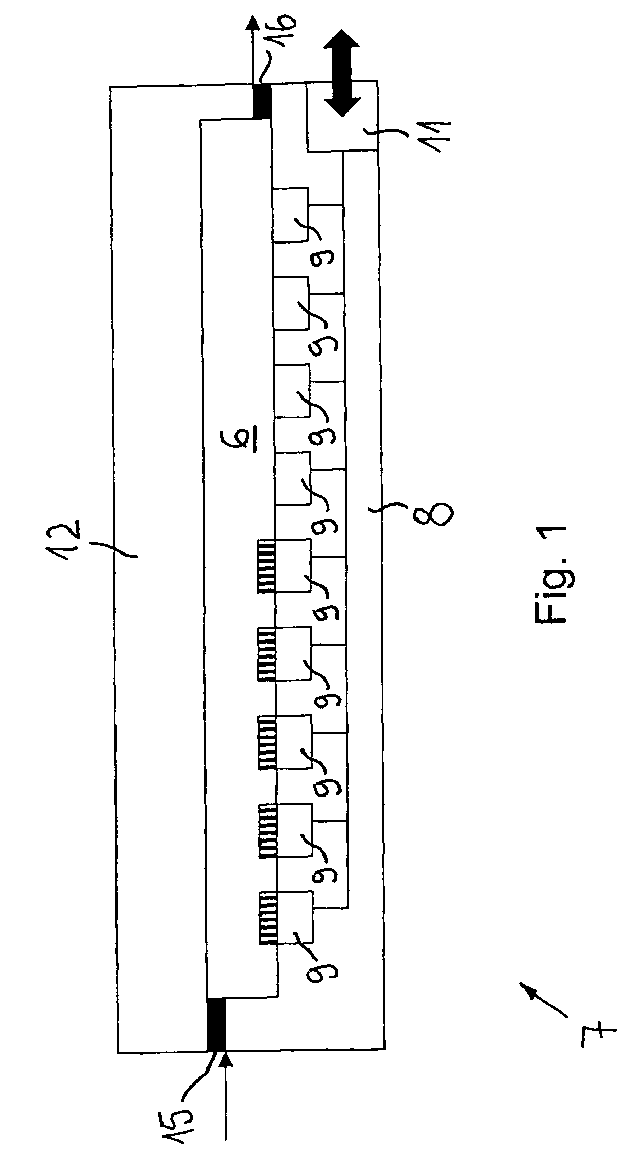
[0020]It is advantageous if there are a plurality of radiation receivers on the semiconductor substrate, preferably in the form of a two-dimensional array, arranged next to one another, and if different receptors are located on the radiation receivers, if necessary. The device then makes it possible to examine analytes for the presence of a number of different ligands.
[0021]It is particularly advantageous if at least two of the different receptors have a different affinity for at least one ligand marked with the luminescent substance, and if, optionally, there are more than two receptors that have a graduated affinity for the at least one ligand. A radiation receiver on which a receptor with a high affinity for the ligand is located then delivers a measurement
signal even at a low concentration of the ligand in an
analyte to be tested in the measurement chamber. A radiation receiver on which a receptor with a
low affinity to the ligand is located delivers a measurement
signal only at a correspondingly higher concentration of the ligand if the measurement
signal from the first above named radiation receiver is already at saturation. A device that has a corresponding number of receptors with graduated affinity thus makes possible a determination of the concentration of the ligands over a
wide dynamic range. The device thereby makes it possible to perform a measurement of the concentration of the ligand with great accuracy both on ligands that are present in a
high concentration and also on ligands that are present in a low concentration, without the requirement for the complex and time-consuming
dilution of the ligand. The receptors can be antibodies that are applied against various epitopes of the same ligand on the individual radiation receivers but have different bonding constants. It is also possible, however, for the affinity of at least one
antibody to be reduced by a
chemical treatment.


