Eureka AIR delivers breakthrough ideas for toughest innovation challenges, trusted by R&D personnel around the world.

Image input system

a technology of input system and output node, which is applied in the field of image input system, can solve the problems of increasing the amount of feedback control performed by the feedback clamping circuit, the unsatisfactory change in the level of the output node, and the undesirable level change in the output period of the charge signal

Inactive Publication Date: 2007-10-09
RENESAS ELECTRONICS CORP +1
View PDF23 Cites 6 Cited by
  • Summary
  • Abstract
  • Description
  • Claims
  • Application Information

AI Technical Summary

Benefits of technology

[0013]The offset voltage due to the capacitive noise component included in the output signal of the solid state image pickup device and the offset cancelling voltage applied to the input terminal of the correlated double sampling amplifier are cancelled out by each other as signal components of polarities opposite to each other by the correlated double sampling amplifier. Consequently, the offset voltage is removed or reduced from the signal information obtained by the solid state image pickup device. Even when the capacitive noise characteristic of the solid state image pickup device is not good, the image input can be performed with high quality.
[0017]The offset cancelling means may comprise as a first mode: offset cancelling voltage generating means for detecting an offset voltage on the basis of an output of the A / D converter in a state where the solid state image pickup device is optically interrupted and generating an offset cancelling voltage on the basis of the detected offset voltage; and second switching means for selectively applying the generated offset cancelling voltage to the reference voltage of the second sampling circuit. Consequently, it is sufficient for the correcting means to execute a feedback clamping control on a signal obtained by eliminating an offset voltage from an output signal of the solid state image pickup device by the offset cancelling voltage. Since it is not necessary to include the amount of signals related to the offset voltage in the amount of a correction control performed by the correcting means, the control amount by the correcting means can be reduced. Even when the correcting means is operated by a low voltage power source, the feedback clamping control can follow satisfactorily.
[0018]The offset cancelling means can comprise as a second mode: a voltage detecting circuit for detecting a signal outputted from the differential amplifier in accordance with the difference voltage between the black level in the feedthrough period in the state where the solid state image pickup device is optically interrupted and the signal level in the charge signal output period; offset voltage generating means for generating an offset cancelling voltage by a difference voltage between the voltage signal detected by the voltage detecting circuit and a reference voltage signal; and second switching means for selectively adding the generated offset cancelling voltage to the reference voltage of the second sampling circuit. In the second mode, in a manner similar to the first mode, the offset voltage can be automatically cancelled by the feedback control. Further, as compared with the first mode, the circuit scale of the offset cancelling means can be reduced more.
[0019]As a third mode, the offset cancelling means may comprise: means for receiving control information for designating the level of the offset cancelling voltage in the state where the solid state image pickup device is optically interrupted from the outside; offset cancelling voltage generating means for generating the offset cancelling voltage on the basis of the received control information; and second switching means for selectively adding the generated offset cancelling voltage to the reference voltage of the second sampling circuit. Although the means does not perform the feedback control, the voltage detecting circuit is unnecessary. Thus, the circuit scale can be reduced.

Problems solved by technology

Due-to parasitic capacitance between the gate and source of the precharge MOS transistor and parasitic capacitance (output node parasitic capacitance) between the final transfer gate of the solid state image pickup device and the output node, when the outputting operation of the outputting unit shifts from the feedthrough period to the charge signal output period, a change in a pulse signal for controlling the charge transfer causes an undesirable change in the level of the output node via the output node parasite capacitance.
The inventors have found that since the capacitance of the floating capacitive element tends to be reduced in order to increase the detection sensitivity of the outputting unit, the output node parasite capacitance relatively increases and it causes an increase in the undesirable level change in the charge signal output period.
The undesirable level change due to the capacitive noise causes an undesirable offset voltage which is outputted from the source follower output circuit in the charge signal output period.
The inventors have found that when the offset voltage increases, the amount of the feedback control performed by the feedback clamping circuit increases and it is feared that the circuit operation cannot follow it.
When the feedback control cannot follow, the reference of the video signal changes at random on the horizontal scan unit basis and it causes unevenness in an input image.
When the conductance of transistors constructing the feedback clamping circuit is increased in order to deal with the problem, it brings about an increase in a chip occupying area and power consumption.
Especially, under the circumstances that the operation source voltage is decreased to realize low power consumption, the necessary feedback control amount cannot be satisfied.
When the preprocessor including the correlated double sampling amplifier and the feedback clamping circuit is provided as a preprocessing LSI formed as a semiconductor integrated circuit, the preprocessing LSI cannot be generally used for a solid state image pickup device having a relatively large capacitive noise component.

Method used


Image

  • Image input system
  • Image input system
  • Image input system

Examples


Embodiment Construction

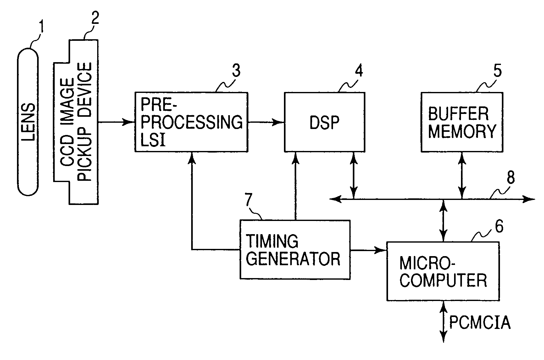
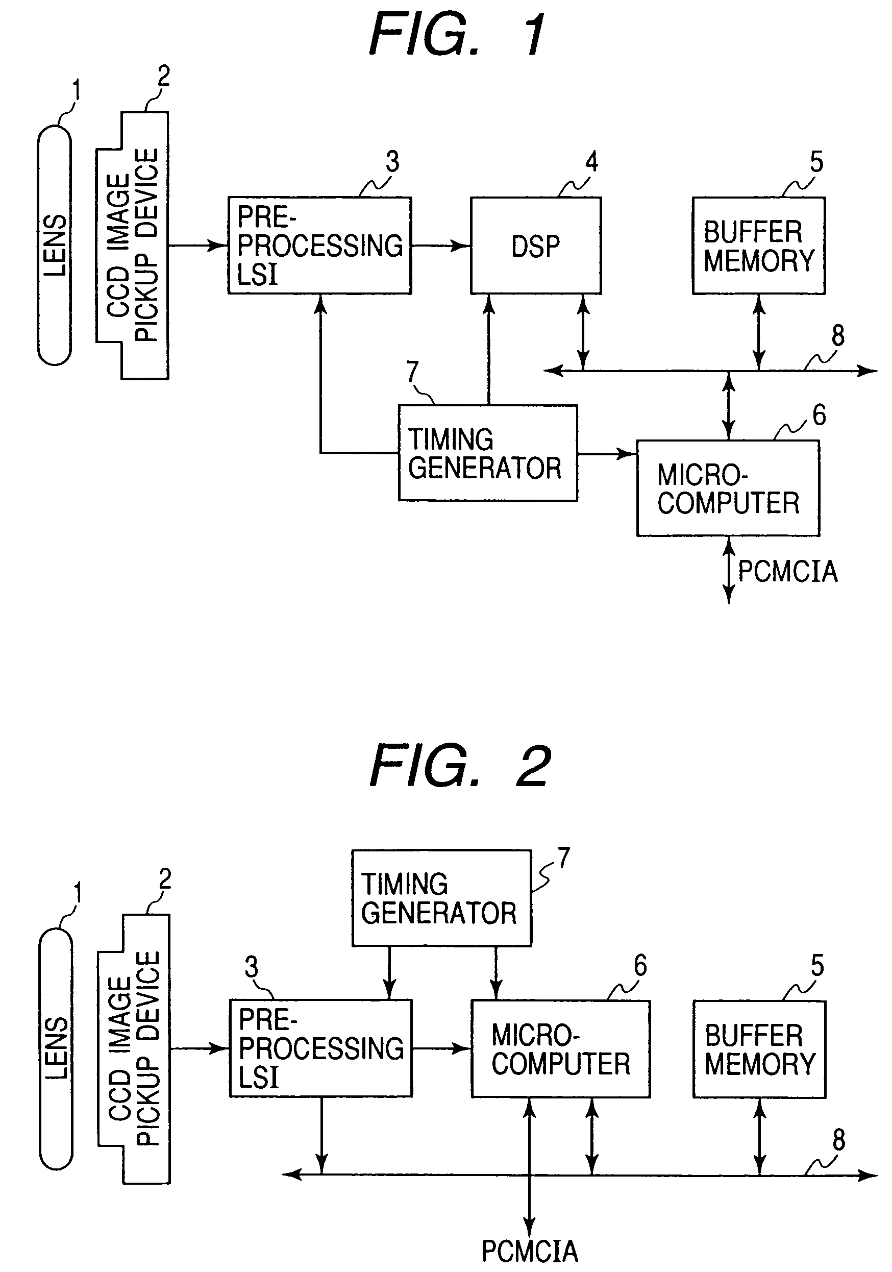
[0033]FIG. 1 shows an embodiment of an image input system according to the invention. The image input system shown in the diagram is applied to a digital video camera, a digital still camera, a digital endoscope, and the like and comprises, as main components, a lens 1, a CCD image pickup device 2, a preprocessor (preprocessing LSI) 3 formed as a semiconductor integrated circuit, a DSP (Digital Signal Processor) 4, a buffer memory 5, a microcomputer 6, and a timing generator 7. Each of the DSP 4 and the microcomputer 6 is an example of a data processor.

[0034]The CCD image pickup device 2 comprises, for example, a photoreceiver having a photoelectric converting function for converting an optical image to a signal charge, a plurality of vertical transfer CCDs for vertically transferring the signal charge photoelectrically converted by the photoreceiver every horizontal line, a horizontal transfer CCD unit for sequentially transferring the charges of each line sent from each of the ver...


PUM


Abstract

An image input system includes a solid state image pickup device and a preprocessor for performing correlated double sampling amplification on an output of the image pickup device and outputting a video signal. The preprocessor has a correlated double sampling amplifier for outputting signal information corresponding to a difference voltage between the black level in a feedthrough period of the image pickup device and a signal level in a charge signal output period; and an offset cancelling circuit for cancelling an offset voltage corresponding to the difference voltage in a state where the image pickup device is optically interrupted to the input terminal of the correlated double sampling amplifier. The correlated double sampling amplifier cancels out the offset voltage and the offset cancelling voltage as signal components of polarities opposite to each other, so that circuits following the correlated double sampling amplifier are not influenced by the offset voltage.

Description

[0001]This is a continuation application of U.S. Ser. No. 10 / 200,162, filed Jul. 23, 2002, now U.S. Pat. No. 6,783,073 which is a continuation application of U.S. Ser. No. 09 / 529,651, filed Apr. 18, 2000, now U.S. Pat. No. 6,499,663.TECHNICAL FIELD[0002]The present invention relates to an image input system for optically inputting an image by using a solid state image pickup device of an X-Y address system using MOS transistors, a solid state image pickup device of a charge transfer system using a CCD (Charge Coupled Device), or the like for photoelectric conversion and charging. More particularly, the invention relates to a technique of lessening an influence of noise components of a signal outputted from a solid state image pickup device, which is exerted on a process of a correlated double sampling method at a post stage or the like and relates to, for example, a technique which is effective when applied to a video camera, a digital still camera or the like.BACKGROUND ART[0003]A ...

Claims


Application Information

Patent Timeline
Patent Type & Authority Patents(United States)
IPC IPC(8): G06F7/10G06K15/12G06K7/10G06K7/14H03G3/32H03K3/00H04N5/20H04N5/357H04N5/361H04N5/363H04N5/365H04N5/378
CPCH04N5/3572H04N5/3575H04N5/378H04N5/3655H04N5/361H04N25/616H04N25/61H04N25/673H04N25/63H04N25/70H04N25/75
Inventor YAHAGI, KOUICHIKASAHARA, MASUMINAKAJIMA, HIROKI
Owner RENESAS ELECTRONICS CORP
Why Eureka
Eureka Blog
Learn More