Conductive adhesive bonded semiconductor substrates for radiation imaging devices

a technology of conductive adhesive and semiconductor substrate, which is applied in the direction of instruments, electrical appliances, radiation measurement, etc., can solve the problems of reducing the mechanical stability of the interconnection, the occurrence of “cold” solder joints, and the above mentioned bump-bonding techniques cannot meet the requirements of new high-density, etc., and achieves cost-effective effects

Active Publication Date: 2007-01-30
OY AJAT LTD
View PDF22 Cites 19 Cited by
  • Summary
  • Abstract
  • Description
  • Claims
  • Application Information

AI Technical Summary

Benefits of technology

[0007]The present invention is a digital radiation imaging device and method for producing the device to digitally image radiation in excess of 1 keV. The imaging device is relatively robust, reliable and cost effective. The present radiation imaging device comprises a semiconductor substrate which generates charge directly in response to incoming radiation, a readout / processing semiconductor substrate for processing and reading out the generated charge, and an electrically conductive adhesive means for joining or bonding the two semiconductor substrates together.

Problems solved by technology

In the field of semiconductor radiation imaging devices comprising a semiconductor detector substrate solder bump-bonded to a semiconductor processing / readout substrate, the occurrence of “cold” solder joints can be a problem.
However, current soldering or the above mentioned bump-bonding techniques cannot fulfill all the requirements of new high-density, imaging device assembly processes which utilize temperature sensitive semiconductor materials in the detector substrates.
This small interconnect area coupled with the relatively more brittle character of some of the promising inter-metallic detector substrates can result in a decrease in the mechanical stability of the interconnection and decreased reliability when solder bump-bonding is used with some of these inter-metallic materials.
Additionally, the use of metallic Lead (Pb) in solder to bond the semiconductor substrates increases the amount of this toxic metal potentially exposed to the environment.

Method used


Image

  • Conductive adhesive bonded semiconductor substrates for radiation imaging devices
  • Conductive adhesive bonded semiconductor substrates for radiation imaging devices
  • Conductive adhesive bonded semiconductor substrates for radiation imaging devices

Examples


Embodiment Construction

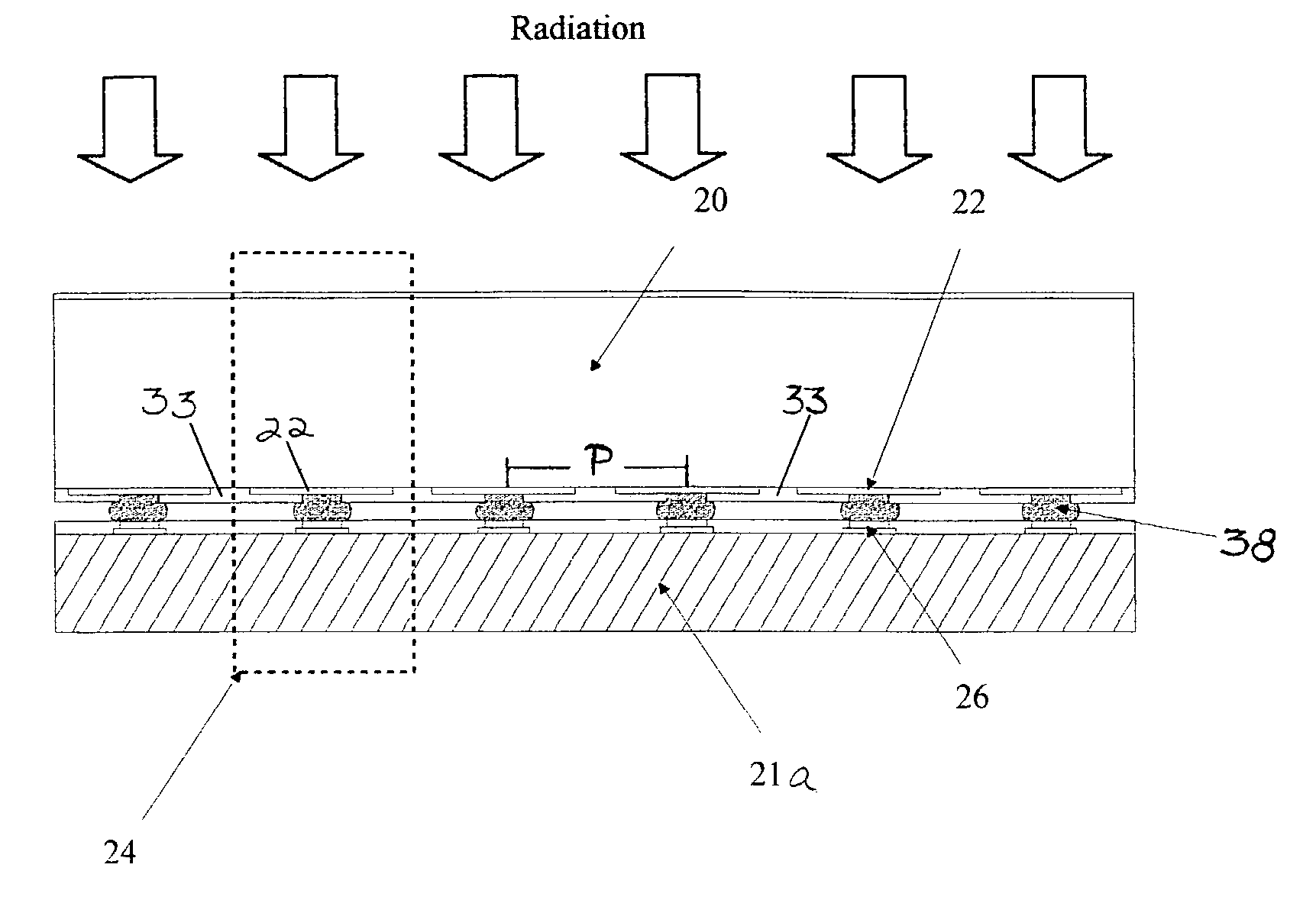
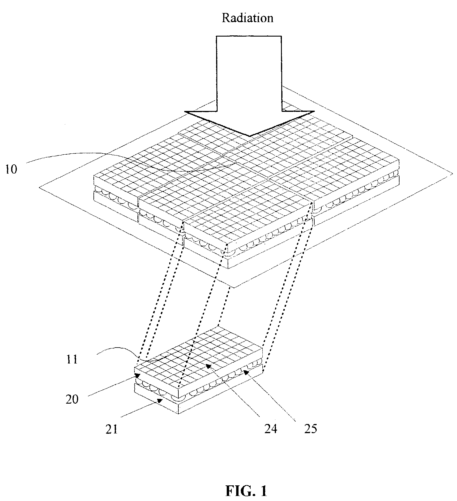
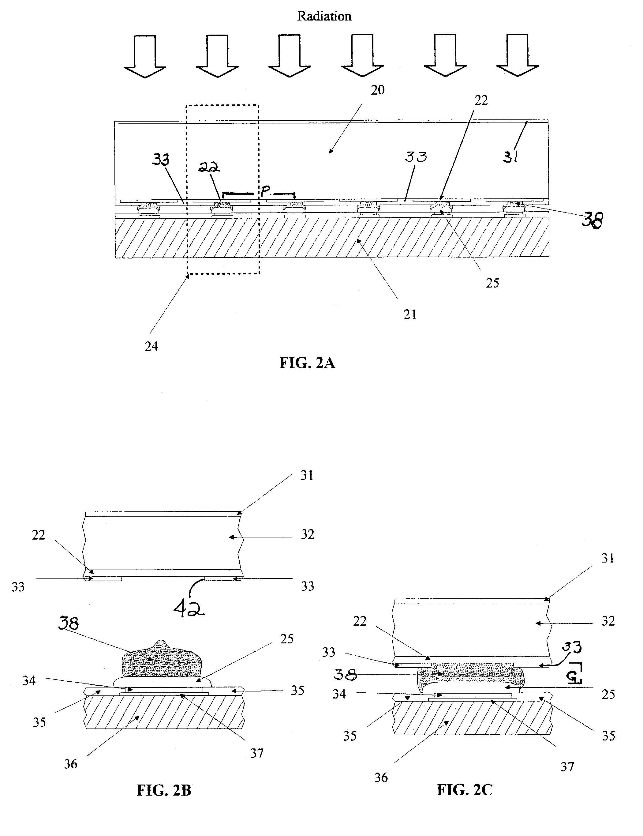
[0045]In accordance with a preferred embodiment of the present invention the radiation imaging device comprises a semiconductor substrate for generating charge directly in response to incoming radiation hits, a readout / processing semiconductor substrate for processing and reading out the generated charge and an isotropically conductive adhesive (ICA) for bonding the two substrates together. Such ICAs have a conductive filler with a high filler loading rate, and they are conductive substantially in all directions equally well. Only a minimum bonding pressure is required when bonding with ICAs. Hence, the brittle CdTe or CdZnTe detector substrates are not subjected to excessive pressure and the risk of damage to the detector substrate is minimized.

[0046]In another preferred embodiment, the imaging device of the present invention comprises a semiconductor substrate for generating charge directly in response to incoming radiation hits, a readout / processing semiconductor substrate for pr...


PUM

PropertyMeasurementUnit
electrically conductiveaaaaaaaaaa
isotropically conductiveaaaaaaaaaa
conductiveaaaaaaaaaa

Abstract

The radiation detector/imaging substrate arrays in an x-ray and gamma-ray radiation energy imaging device are described which use an electrically conductive adhesive to provide electron charge signaling continuity between the detector and read-out substrates of the device. The present device utilizes a plurality of electrically conductive bonds each discretely connecting a pixel contact in the pixel pattern to a signal contact in the signal contact pattern, the bonds being an electrically conductive adhesive. This bonding technique is especially useful in detection/imaging arrays having detector substrates comprising Cadmium and Tellurium compositions. The present invention is practicable with semiconductor detector and read-out substrates with or without “bumped” electrical contacts. The electrically conductive bonds utilize either isotropically or anisotropically conductive adhesives.

Description

[0001]The present application claims the benefit of prior filed U.S. Provisional Application, Ser. No. 60 / 368,540, filed 29 Mar. 2002, to which the present application is a non-provisional U.S. Patent Application, and the content of which is incorporated herein by reference.FIELD OF THE INVENTION[0002]The present invention is in the field of semiconductor devices for detecting invisible radiant energy. More specifically, the present invention relates to imaging systems for forming an image of an object and having detection means including a Cadmium Telluride substrate bonded to a specific semiconductor arrangement using a conductive adhesive.BACKGROUND OF THE INVENTION[0003]In the field of semiconductor radiation imaging devices comprising a semiconductor detector substrate solder bump-bonded to a semiconductor processing / readout substrate, the occurrence of “cold” solder joints can be a problem. See U.S. Pat. Nos. 5,379,336; 5,812,191; EP 1162833; and EP 0421869. Cold solder joints...

Claims


Application Information

Patent Timeline
Patent Type & Authority Patents(United States)
IPC IPC(8): G01T1/24H01L21/00H01L25/065H01L27/146G01N23/04G01T1/161H01L27/00
CPCH01L27/14634H01L27/14658H01L27/1469H01L27/14661H01L27/14696H01L27/14694G01T1/24H01L31/101
Inventor VUORELA, MIKKO ILMARI
Owner OY AJAT LTD
Why Eureka
Try Eureka