
Method of manufacturing a TFT with laser irradiation

a thin film transistor and laser irradiation technology, applied in the direction of transistors, electrical devices, semiconductor devices, etc., can solve the problems of uniform quality of tfts thus obtained, and achieve the effects of uniform device characteristics, high yield and high resistan

Inactive Publication Date: 2007-01-23
SEMICON ENERGY LAB CO LTD
View PDF114 Cites 3 Cited by
  • Summary
  • Abstract
  • Description
  • Claims
  • Application Information

AI Technical Summary

Benefits of technology

The present invention provides a method for fabricating TFTs with uniform device characteristics by forming high resistance regions in a self-alignment process without using photolithography. The high resistance regions are formed by selectively introducing nitrogen or other impurities into the active layer using a gate insulating film and a gate electrode as masks. The thickness of the gate insulating film can be precisely controlled, and the high resistance regions can be formed without causing fluctuation in their width. The method improves mass production of TFTs and ensures the formation of high resistance regions with higher certainty.

Problems solved by technology

Thus, it is difficult to form high resistance regions on the edge portion of the gate electrode in a self-alignment; hence, the TFTs are fabricated at a low yield, and moreover, the TFTs thus obtained are not uniform in quality.

Method used


Image

  • Method of manufacturing a TFT with laser irradiation
  • Method of manufacturing a TFT with laser irradiation
  • Method of manufacturing a TFT with laser irradiation

Examples


example 1

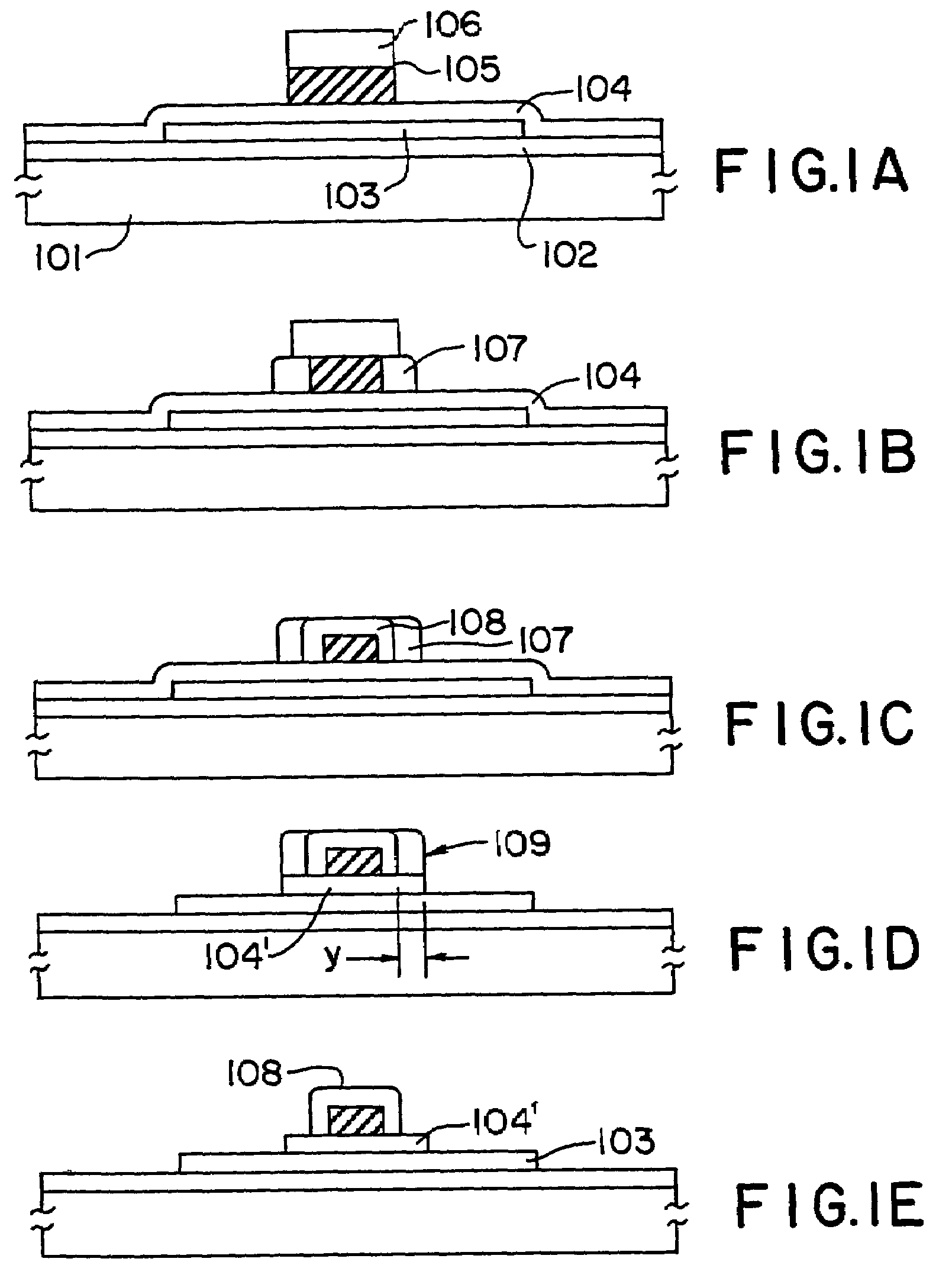
[0034]A silicon oxide film having a thickness of 1,000 to 3,000 Å is formed as a base oxide film 102 on a Corning 7059 substrate 101 (300×400 mm or 100×100 mm in size) by sputtering in an oxygen atmosphere. For mass production, the film is deposited by decomposing TEOS using plasma CVD. A mono-layered film of aluminum nitride or a multilayered film of silicon oxide and aluminum nitride can be used as the base oxide film. The aluminum nitride film is formed by reactive sputtering in a nitrogen atmosphere.

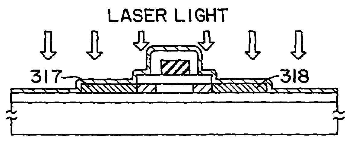
[0035]An amorphous silicon film is deposited thereafter at a thickness of 300 to 5,000 Å, preferably, 500 to 1,000 Å, by plasma CVD or LPCVD, and is crystallized thereafter by allowing it to stand still in a reduction atmosphere in a temperature range of 550 to 600° C. for 24 hours. The crystallization may be effected by laser irradiation. Thus crystallized silicon film is patterned to form an island-like region 103. A silicon oxide film 104 having a thickness of 700 to 1,500 Å is fo...

example 2

[0049]A base film 102, an active layer 103, a gate insulating film 104′, a gate electrode 105, and an anodic oxide 108 are formed on a glass substrate 101 by processes similar to that described in Example 1 (FIG. 1E).

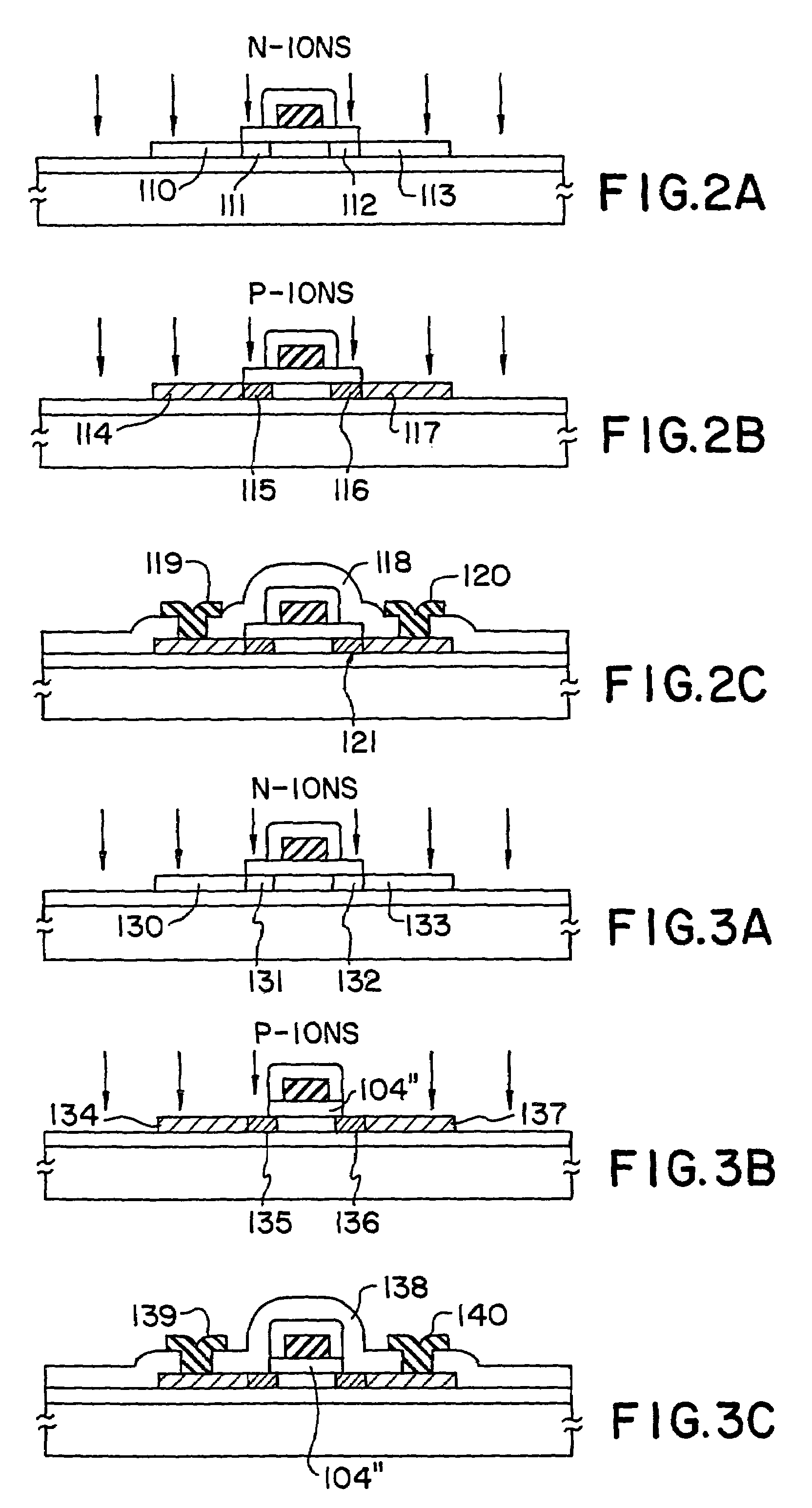
[0050]Nitrogen ions are introduced in a self-alignment into the active layer 103 using the gate electrode and the gate insulating film as masks. The dose is 1×10¹⁴ to 3×1016 cm−2, for example, 2×1015 cm−2. An accelerating voltage is 50 to 100 kV, for example, 80 kV. As a result, almost no nitrogen atoms are introduced into the regions 130 and 133 (the concentration of nitrogen is 1×10¹⁹ atoms cm−3 or less in SIMS), but nitrogen atoms are introduced into the regions 131 and 132 at a concentration of 5×10¹⁹ to 2×10²¹ atoms cm−3 depending on the depth (FIG. 3A).

[0051]The gate insulating film 104′ is etched thereafter to form a gate insulating film 104″ by using the anodic oxide 108 as a mask. An N-type impurity is introduced into the active layer thereafter by ion doping a...

example 3

[0054]Referring to FIGS. 5A to SF, a method for fabricating an N-channel TFT is described below. First referring to the processes shown in FIGS. 1A and 1B, a base oxide film 202, an island-like semiconductor (e.g., a crystalline silicon semiconductor) region 203, a silicon oxide film 204, and a gate electrode 205 comprising an aluminum film (200 nm to 1 μm in thickness) are formed on a substrate 201 having an insulating surface (e.g., a Corning 7059 glass), and a porous anodic oxide 206 (3,000 Å to 1 μm in thickness, e.g., 5,000 Å) is formed in both sides of the gate electrode 205 (FIG. 5A).

[0055]A barrier anodic oxide 207 (1,000 to 2,500 Å in thickness) is formed thereafter in the same manner as in the process described in Example 1 (FIG. 5B).

[0056]The silicon oxide film 204 is etched using the anodic oxide 206 as the mask, to form a gate insulating film 204′. Then, the anodic oxide film 206 is removed by etching using the anodic oxide film 207 as the mask. Impurity (phosphorus) is...


PUM

PropertyMeasurementUnit
distanceaaaaaaaaaa
glass transition temperatureaaaaaaaaaa
thicknessaaaaaaaaaa

Abstract

In a thin film transistor (TFT), a mask is formed on a gate electrode, and a porous anodic oxide is formed in both sides of the gate electrode using a relatively low voltage. A barrier anodic oxide is formed between the gate electrode and the porous anodic oxide and on the gate electrode using a relatively high voltage. A gate insulating film is etched using the barrier anodic oxide as a mask. The porous anodic oxide is selectively etched after etching barrier anodic oxide, to obtain a region of an active layer on which the gate insulating film is formed and the other region of the active layer on which the gate insulating film is not formed. An element including at least one of oxygen, nitrogen and carbon is introduced into the region of the active layer at high concentration in comparison with a concentration of the other region of the active layer. Further, N- or P-type impurity is introduced into the active layer. Accordingly, high resistance impurity regions are formed in both sides of a channel forming region.

Description

BACKGROUND OF THE INVENTION[0001]1. Field of the Invention[0002]The present invention relates to an insulated gate thin film transistor formed on an insulating material (e.g., glass) or a material such as a silicon wafer having thereon an insulating film (e.g., silicon oxide), and to a method for fabricating the same. The present invention is particularly effective for thin film transistors fabricated on a glass substrate having a glass transition temperature (deformation temperature or deformation point) of 750° C. or less. The thin film transistor according to the present invention is useful for driver circuits of, for example, active matrix liquid crystal displays and image sensors, as well as for three dimensional integrated circuits.[0003]2. Description of the Related Art[0004]Thin film transistors (referred to simply hereinafter as “TFTs”) are widely employed for driving, for example, liquid crystal displays of active matrix type and image sensors. TFTs of crystalline silicon ...

Claims


Application Information

Patent Timeline
Patent Type & Authority Patents(United States)
IPC IPC(8): H01L21/00H01L21/336H01L21/77H01L21/84H01L29/786
CPCH01L27/1214H01L29/78618H01L29/66757H01L27/1296H01L27/127
Inventor ZHANG, HONGYONGOHNUMA, HIDETOYAMAGUCHI, NAOAKITAKEMURA, YASUHIKO
Owner SEMICON ENERGY LAB CO LTD
Learn More