Semiconductor switches and switching circuits for microwave

a technology of switching circuits and switches, applied in the field of microwave-based switches, can solve the problems of reducing yield, increasing loss due to reflection, and practicably difficult to maintain low insertion loss, and achieve high isolation. , the effect of reducing the resistance “r”

Inactive Publication Date: 2006-11-14
RENESAS ELECTRONICS CORP
View PDF7 Cites 0 Cited by
  • Summary
  • Abstract
  • Description
  • Claims
  • Application Information

AI Technical Summary

Benefits of technology

[0036]As described above, in the switching circuit functioning as a coplanar line without loss and with loss respectively in the ON state and in the OFF state, the 0th digit close resemblance on the isolation frequency is expressed by the equation (10). In addition, as being understood from this equation, larger isolation may be obtained by reducing the resistance “r”, which is as mentioned before.
[0037]Qualitatively, with a constant sheet resistance value, wider width of an element reduces the resistance value, and longer length of an element increases the resistance value, which is generally known.
[0038]Here, with the width of an FET being constant, comparison between the switching circuits of Conventional example 3 and semiconductor switches and switching circuits according to the present invention leads to the following understanding. That is, the resistance value of the distributed parameter FET in Conventional example 3 is already defined by the source-drain distance. On the contrary, the resistance values of the resistance defining isolation in the switches according to the present invention depend on the gate-source, and the gate-drain distances. In detail, a switch according to the present invention comprises such a configuration that the source, the gate, and the drain of a so-called Schottky barrier FET are enclosed by an active layer, and the source as well as the drain is connected with the earth. Thus, when forward bias voltage which is to determine the current value to flow to the gate by the source-drain resistance is supplied as gate voltage to between the gate and source as well as between the gate and the drain, the resistance which determines the isolation in the switches of the present invention is understood to be the source resistance between the gate and the source or the drain resistance between the gate and the drain of Schottky barrier diode. That is, unlike Conventional example 3, in the switches according to the present invention, the resistance value to determine isolation is determined by distances between gate and source as well as between gate and drain. This leads to understanding that the resistance value of the resistance to determine isolation in the switches of the present invention is simply considered to be decreased to approximately a half of that of Conventional example 3 since the gate electrode of an FET to be used for switches is disposed in general in the middle between the source and the drain. Incidentally, for easier understanding, the contact resistance is set to be constant. As understandable from the foregoing, the semiconductor switches according to the present invention can realize compactness as well as lower loss, and high isolation when compared with not only Conventional examples 1 and 2 but also Conventional example 3.

Problems solved by technology

As a result, a signal pass where a diode is biased in the reverse direction allows signals to travel transparently, but on the other hand, an increase in frequency will result in an increase in loss due to reflection.
On the contrary, FETs as well as PIN diodes, etc., normally have variation of forming process to a certain extent, but for example, due to this variation, the value of capacitance C could deviate from the design, and as a result the resonance frequency will deviate from the design as well, and resonance will not be available at a desired frequency, which, as a consequence, will give rise to reduction of yield.
However, not only in switching circuits of the above-described Conventional example 1 as well as Conventional example 2 without doubt, but also in switching circuit of Conventional example 3 it was practically difficult to maintain low insertion loss and realize high isolation in a wide band as a comparatively compact type.
As understandable from these features, in microwave or millimeter wave band switching circuits there was a problem that it was difficult for the prior art to realize high isolation of not less than 80 dB covering a wide band width with a comparatively small type configuration, while maintaining low insertion loss.

Method used


Image

  • Semiconductor switches and switching circuits for microwave
  • Semiconductor switches and switching circuits for microwave
  • Semiconductor switches and switching circuits for microwave

Examples


first embodiment

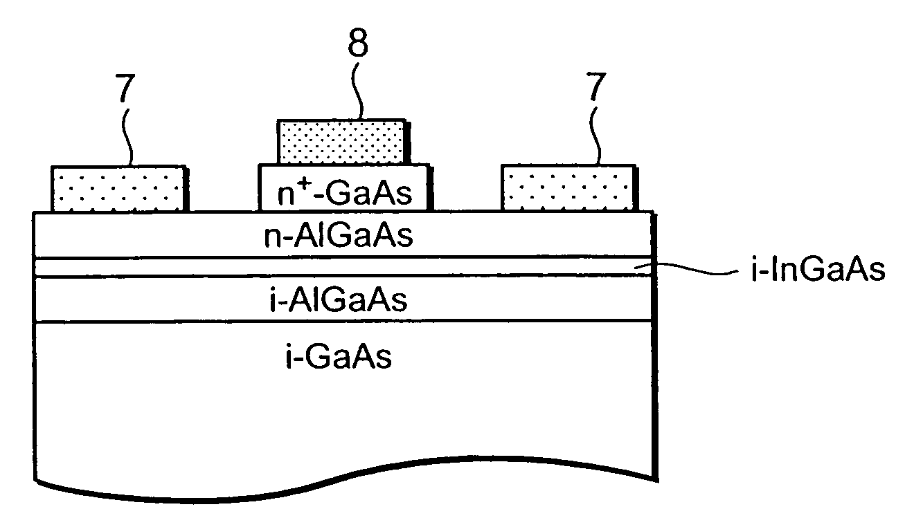
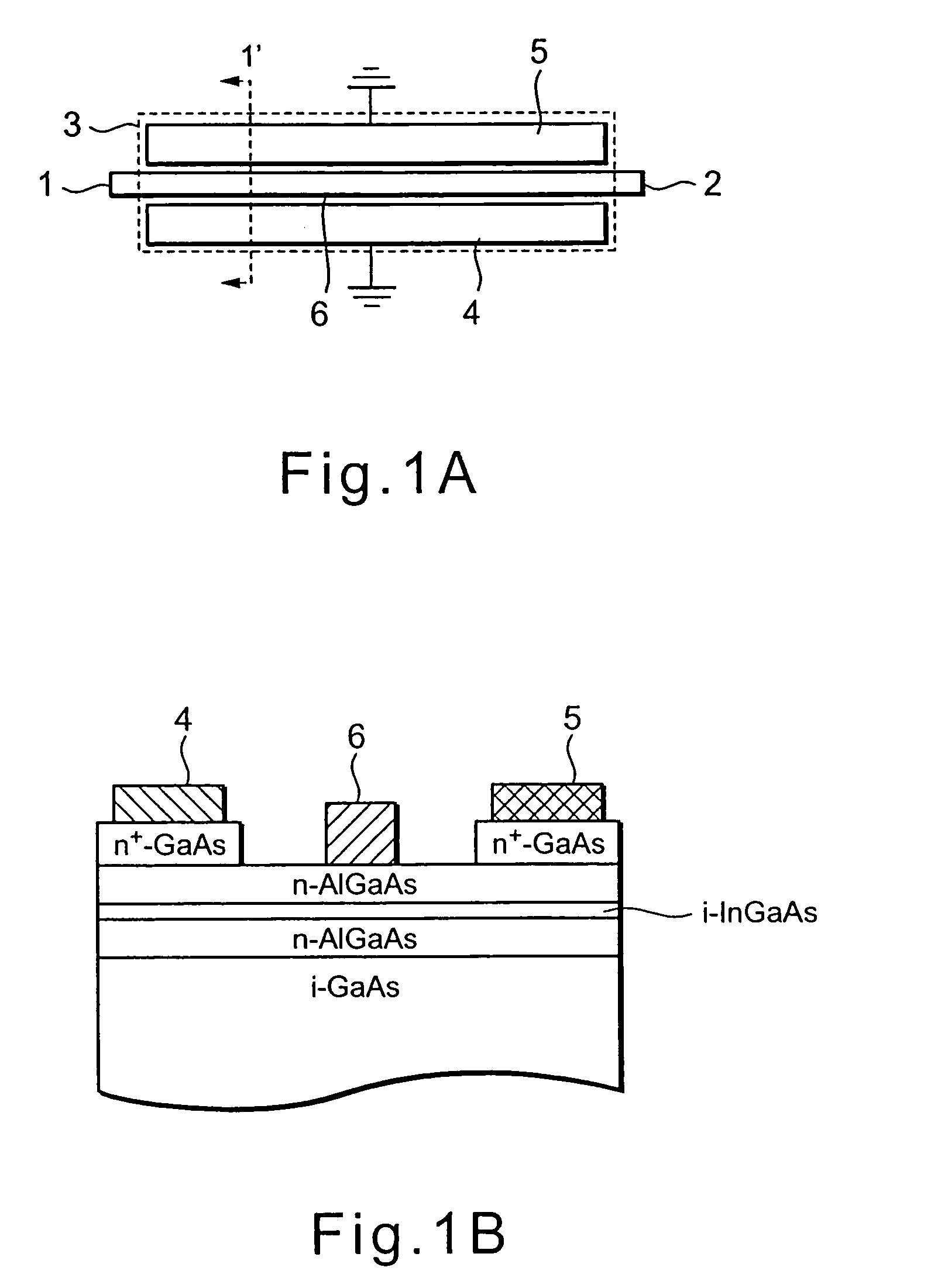
[0067]In the present example, a heterojunction FET of AlGaAs and InGaAs systems was used as the FET in the above-described In detail, referring to FIG. 1B, a n-AlGaAs layer is formed on an i-GaAs layer. An i-InGaAs layer as a channel layer is formed on the n-AlGaAs layer. A n-AlGaAs layer is formed on the i-InGaAs layer. 2 n+-GaAs layers are formed on the n-AlGaAs layer apart from each other. The gate electrode 6 is formed on the n-AlGaAs layer between the n+-GaAs layers. The gate electrode 6 is made by aluminum, gold, molybdenum, titanium, or tungsten silicide. The source electrode 4 is formed on one of the n+-GaAs layer. The drain electrode 5 is formed on the other of the n+-GaAs layer. The source and drain electrodes are made by an alloy including AuGe or nickel. In addition, the area of the gate electrode 6 was set to 2×400 μm, and the distances between the gate electrode 6 and the source electrode 4 or the drain electrode 5 were set to 2.5 μm. Moreover, the first input-output ...

third embodiment

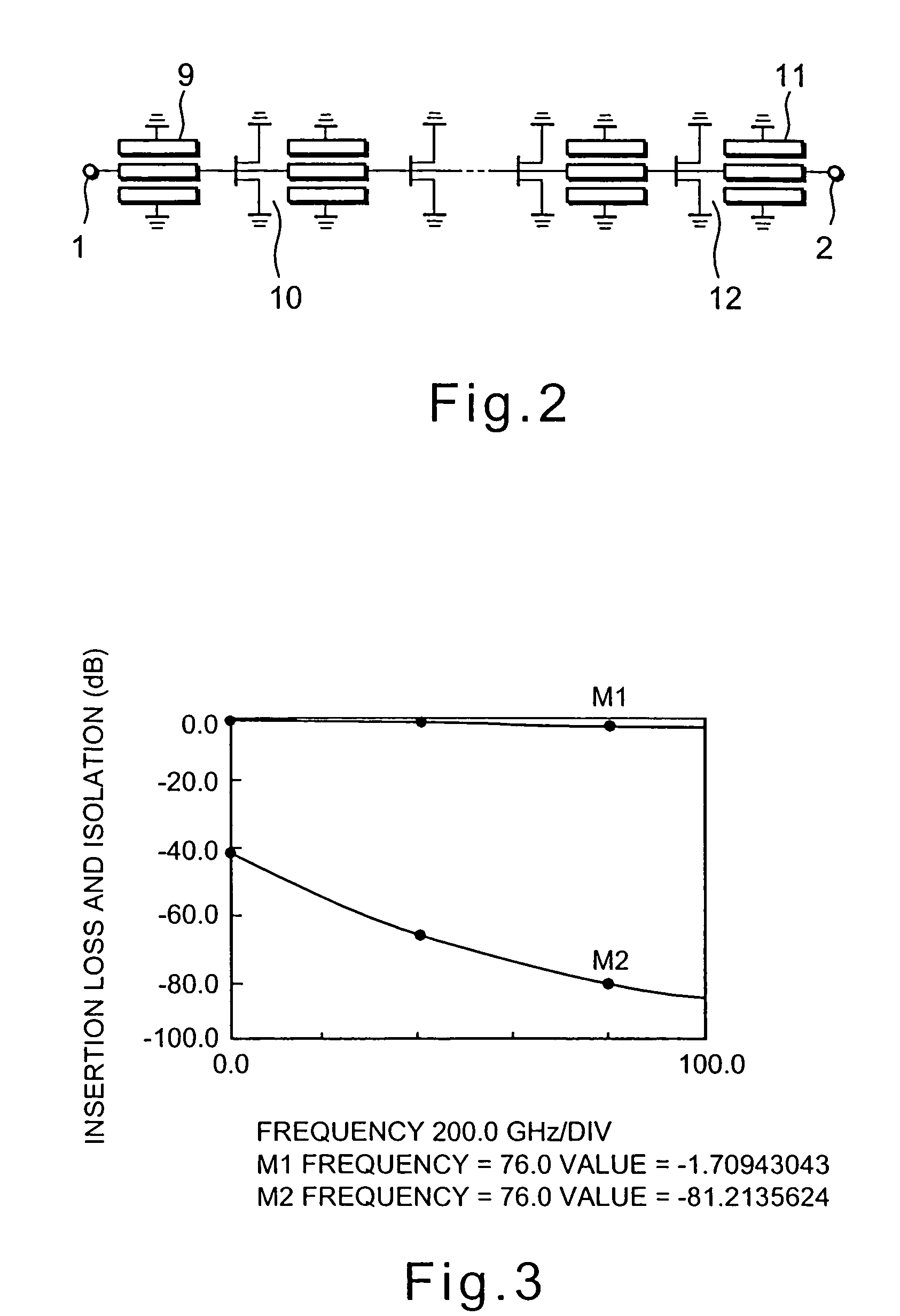
[0086]FIG. 11 is a graph showing frequency characteristics on insertion loss as well as isolation of the semiconductor switch according to the other example in correspondence with the In the present example, the area of the anode electrode 7 was set to 10×400 vm, and the distance between the cathode electrode 8 and the anode electrode 7 was set to 2.5 μm. In addition, the first input-output terminal 1 and the second input-output terminal 2 are respectively connected with both the ends of the anode electrode 7, and further, 50 Ω loads are respectively connected with the first input-output terminal 1 and the second input-output terminal 2. Capacitance with zero bias between the cathode and the anode is 20 fF per 100 μm, and on the other hand, resistance with forward bias is 3.3 Ω per 100 μm. In addition, entire length of the coplanar line is 400 μm.

[0087]In the semiconductor switch according to the present example comprising such configuration, unlike the foregoing example, the case ...


PUM


Abstract

The purpose of the present invention is to provide a small-sized switch attaining high isolation of not less than 80 dB, maintaining low insertion loss also in high frequencies not less than 60 GHz. A semiconductor switch according to the present invention utilizes FETs a gate electrode, a source electrode, and a drain electrode of each of which are formed on a semiconductor. The source electrode and the drain electrode are connected with the earth as well as are disposed in parallel to each other, and the gate electrode is formed between the source electrode and the drain electrode, and both the ends of the gate electrode are connected to the first input-output terminal 1 and the second input-output terminal.

Description

CROSS REFERENCE TO RELATED APPLICATIONS[0001]This application is a continuation of U.S. patent application Ser. No. 09 / 372,322 filed Aug. 11, 1999 now abandoned.BACKGROUND OF THE INVENTION[0002]1. Field of the Invention[0003]This invention relates to semiconductor switches, and in particular to semiconductor switches for microwave as well as millimeter wave bands using a transmission line comprising a dielectric substance substrate and metal conductors, and diodes or field effect transistors (FETs) showing distributed parameter effect.[0004]2. Description of the Prior Art[0005]As a semiconductor switching circuit which is contemplated for use in microwave as well as millimeter wave bands, in particular with high frequencies not less than 60 GHz, various kinds of circuits have been proposed and manufactured for trial.[0006]Single-pole 3-throw (SP3T) switches for the 77 GHz band (hereinafter to be referred to as Conventional example 1) were reported by M. Case et al. in “1997 MTT-S IM...

Claims


Application Information

Patent Timeline
Patent Type & Authority Patents(United States)
IPC IPC(8): H01L31/0328H01L29/872H01L27/095H01L29/47H01L29/861H01P1/15H01P3/02
CPCH01L29/7783H01P1/15
Inventor MIZUTANI, HIROSHI
Owner RENESAS ELECTRONICS CORP
Why Eureka
Try Eureka