Semiconductor integrated circuit including a DRAM and an analog circuit

Inactive Publication Date: 2006-10-10
FUJITSU SEMICON LTD
View PDF14 Cites 4 Cited by
  • Summary
  • Abstract
  • Description
  • Claims
  • Application Information

AI Technical Summary

Benefits of technology

[0016]Another object of the present invention is to provide a semiconductor device including a memory cell region, in which a memory cell capacitor is formed, and a peripheral region where no such a memory cell capacitor is formed, wherein the problem of irregular polysilicon pattern remaining at a stepped part formed between the memory cell region and the peripheral region is effectively eliminated.
[0017]Another object of the present invention is to provide a fabrication process of a semiconductor device that includes a memory cell region, in which a memory cell capacitor is formed, and a peripheral region where no such a-memory cell capacitor is formed, wherein a capacitor is formed in the peripheral region without increasing the number of the mask steps.
[0023]According to the present invention, the problem of etching of the second region, which tends to occur in the semiconductor device that has the first region, or memory cell region, including therein a capacitor and further the second region or a peripheral region, when patterning the capacitor in the first region, is successfully avoided by protecting the second region by a mask process during the foregoing patterning process of the capacitor. As a result, the height of the stepped part formed between the first region and the second region, which otherwise would be formed with a substantial step height, is successfully minimized. Further, by covering the stepped part between the first region and the second region by a conductive pattern, the problem associated with the formation of conductive residue at such a stepped part such as peeling and scattering of the conductive residue is effectively avoided. Further, by forming the capacitor insulation film concurrently with the side wall insulation film of the contact hole formed in the memory cell region, it becomes possible to form a large-capacitance capacitor without increasing the area of the semiconductor device or increasing the number of the mask steps. Further, by forming a dummy memory cell capacitor in the marginal part of the memory cell region such that the edge part of the storage capacitor covers, on the field oxide film, an insulation film identical with the insulation film forming a side wall insulation film of the contact holes for other memory cell capacitors, the problem of unnecessary increase in the area associated with the formation of the dummy memory cell is effectively avoided.
[0032]According to the present invention, it becomes possible, in a semiconductor device in which an analog circuit device having a capacitor and another semiconductor circuit are formed monolithically on a common substrate, to eliminate the problem of pinhole formation in a side wall insulation film that protects a side wall of a contact hole, even in such a case in which a native oxide film is removed from the surface of the substrate exposed by the contact hole by applying a wet etching process using HF, and the like, by providing a conductive layer on the side wall insulation film covering the side wall of the contact hole. The present invention is particularly useful when forming the capacitor in the analog circuit device concurrently with the side wall insulation film, as the conductive layer effectively protects the capacitor insulation film. Thereby, the problem of thinning of the capacitor insulation film or formation of pinhole in the capacitor insulation film is positively eliminated. As the capacitor insulation film and the side wall insulation film of the contact hole are formed simultaneously by the common process, and as the conductor layer on the side wall insulation film and the conductor layer protecting the capacitor insulation film are formed simultaneously by the common process, there occurs no increase in the number of the mask steps.
[0045]According to the present invention, it becomes possible to form, in a semiconductor integrated circuit in which two or more, different semiconductor circuits such as a DRAM and an analog circuit are formed, the capacitor of the analog circuit and the bit line contact or bit line pattern of the DRAM without increasing the number of the mask steps.

Problems solved by technology

The DRAM 10 of FIG. 1, however, has suffered from a drawback in that there tends to appear a large step height between the memory cell region 10A and the peripheral region 10B as a result of the repeated etching processes for forming the memory cell capacitors in the memory cell region 10A.
Further, such a stepped part at the boundary of the memory cell region 10A and the peripheral region 10B tends to invite accumulation of irregular polysilicon residue, which may cause various unpreferable effects such as short-circuit.

Method used


Image

  • Semiconductor integrated circuit including a DRAM and an analog circuit
  • Semiconductor integrated circuit including a DRAM and an analog circuit
  • Semiconductor integrated circuit including a DRAM and an analog circuit

Examples


first embodiment

[First Embodiment]

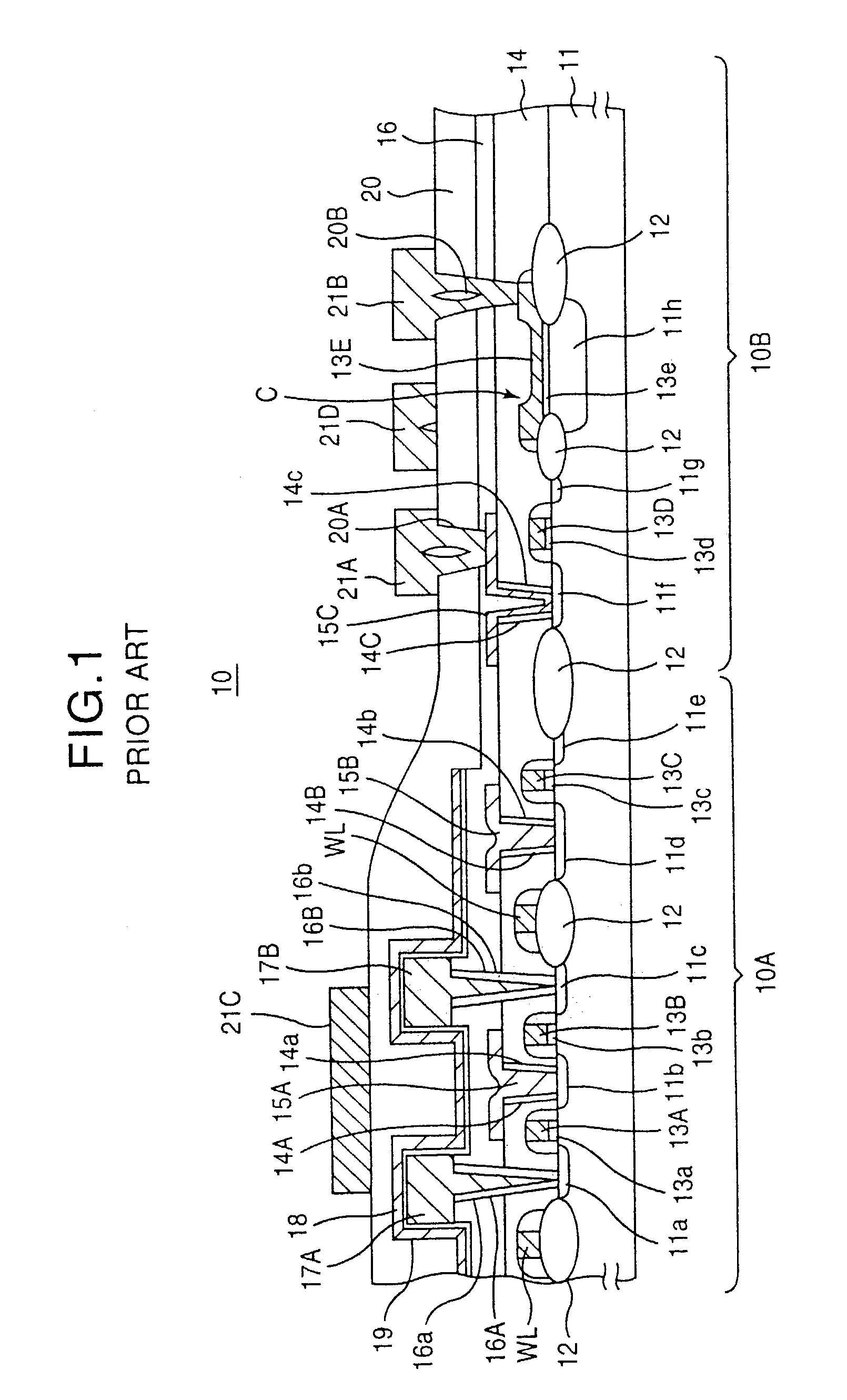
[0069]FIGS. 2A–2C show the process of forming the memory cell capacitor in the semiconductor device of FIG. 1 according to a first embodiment of the present invention, wherein those parts corresponding to the parts described previously are designated by the same reference numerals and the description thereof will be omitted.

[0070]Referring to FIG. 2A, the contact hole 16B is formed in the second interlayer insulation film 16 so as to expose the diffusion region 11c, and an insulation film 16′ is deposited on the interlayer insulation film 16 so as to cover the side wall of the contact hole 16B. Next, in the step of FIG. 2B, an anisotropic etching process acting substantially perpendicularly to the principal surface of the substrate 11 is applied on the insulation film 16′, and the side wall insulation film 16b is formed by removing the insulation film 16′ remaining on the interlayer insulation film 16.

[0071]Next, in the step of FIG. 2B, a polysilicon film is deposi...

second embodiment

[Second Embodiment]

[0074]FIGS. 3A–3F show the fabrication process of a DRAM according to a second embodiment of the present invention wherein the problems of the first embodiment is eliminated.

[0075]Referring to FIG. 3A, a p-type Si substrate 31 is formed with an n-type well 31A and an initial oxide film (not shown) is formed on the substrate with a thickness of about 3 nm. Further, an SiN pattern 32 is formed thereon with a thickness of about 115 nm, such that the SiN pattern 32 defines a device isolation region.

[0076]Next, in the step of FIG. 3B, field oxide films 33A–33F are formed on the substrate 31 by a wet oxidation process with a thickness of about 320 nm while using the SiN pattern 32 as a mask. Further, a p-type well 31A is formed in the n-type well 31A in correspondence to the memory cell region 30A by conducting an ion implantation process of B+. Further, there is formed a p-type well 31C in the substrate 31 in correspondence to a peripheral region 30B formed outside the...

third embodiment

[Third Embodiment]

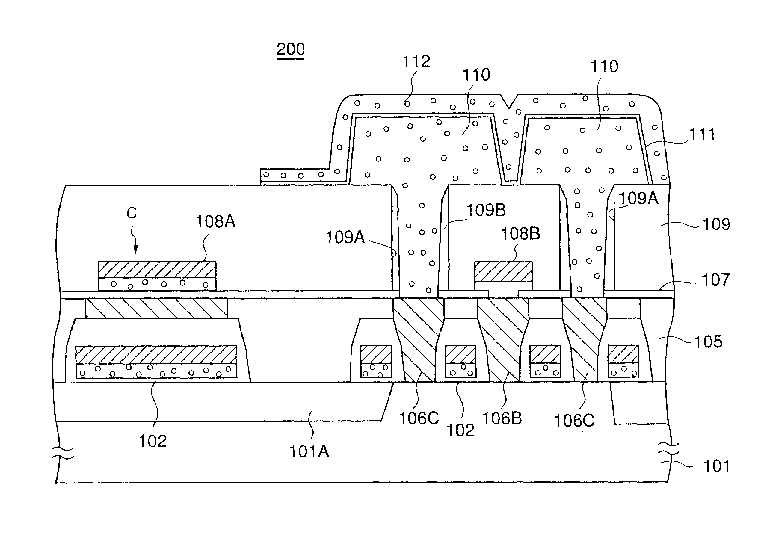
[0097]In the DRAM of the previous embodiment, there can be a case in which the conductor layer constituting the storage electrode 41 or the opposing electrode 43 remains unetched along the stepped part S3 between the memory cell region 30A and the peripheral region 30B as an irregular pattern 42X at the time of the patterning of the storage electrode 41 or the opposing electrode 43 as represented in FIG. 6.

[0098]FIGS. 7A and 7B show the formation of the memory cell capacitor in the memory cell region 30A in a plan view, wherein FIG. 7A corresponds to the step of FIG. 4B.

[0099]Referring to FIG. 4A, there is formed a stepped part S1 at the outer side of the memory cell region 30A represented by the broken line as a result of the patterning process conducted by the resist pattern 40, and contact holes 30A are formed in the memory cell region 30A in a row and column formation.

[0100]On the other hand, FIG. 4B corresponds to the foregoing step of FIG. 4D and shows the st...


PUM


Abstract

A semiconductor device including an interlayer insulation film formed on a substrate so as to cover first and second regions defined on the substrate, and a capacitor formed over the interlayer insulation film in the first region, wherein the interlayer insulation film includes, in the first region, a stepped part defined by a groove having a bottom surface lower in level than a surface of the interlayer insulation film in the second region.

Description

[0001]This application is a divisional of prior application Ser. No. 09 / 397,502 filed Sep. 17, 1999 now U.S. Pat. No. 6,583,458BACKGROUND OF THE INVENTION[0002]1. Field of the Invention[0003]The present invention generally relates to semiconductor devices and more particularly to a semiconductor device having a capacitor and a fabrication process thereof.[0004]2. Description of the Related Art[0005]A DRAM is a high-speed semiconductor memory device that stores information in a capacitor formed therein monolithically in the form of electric charges. Thus, DRAMs are used extensively in information processing apparatuses such as a computer as a memory device.[0006]In these days, there is a demand for a semiconductor device in which a DRAM and an analog circuit device are formed monolithically on a common semiconductor substrate. Such an analog circuit device generally includes a capacitor formed in the monolithic state.[0007]FIG. 1 shows the construction of a conventional DRAM 10.[0008...

Claims


Application Information

Patent Timeline
IPC IPC(8): H01L21/8242H01L27/06H01L21/02H01L21/8234H01L27/108
CPCH01L27/10894H01L27/1052H01L27/10852H01L28/90H01L2924/0002H01L2924/00H10B12/033H10B12/09H10B12/00H10B99/00
Inventor HAYASHI, LEGAL REPRESENTATIVE, TADAAKIEMA, TAIJIOHKAWA, NARUMIHAYASHI, DECEASED, MASAO
Owner FUJITSU SEMICON LTD
Why Eureka
Try Eureka