
High speed cross-point switch using SiGe HBT technology

a high-speed cross-point switch and hbt technology, applied in the field of high-speed cross-point switches, can solve the problems of reducing the theoretical insertion loss of a high-frequency cross-point switch, and affecting the operation of the high-frequency passive cross-point switch. , to achieve the effect of reducing the theoretical insertion loss, reducing the concentration of electric fields, and increasing the dielectric loss

Inactive Publication Date: 2006-01-10
COBHAM DEFENSE ELECTRONICS SYST CORP
View PDF5 Cites 4 Cited by
  • Summary
  • Abstract
  • Description
  • Claims
  • Application Information

AI Technical Summary

Benefits of technology

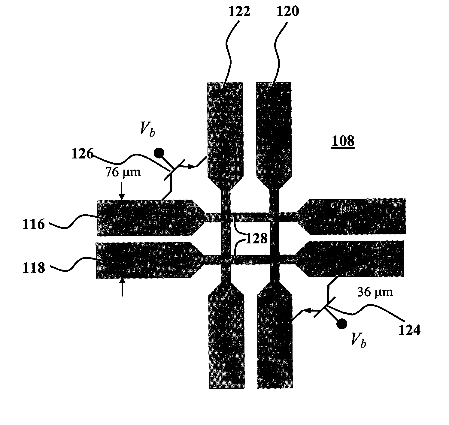
[0009]During the last few years, SiGe technology has been increasingly used for high frequency applications. Although the silicon substrate has significantly higher dielectric loss than GaAs substrate, we have discovered that use of appropriate transmission lines that allow less concentration of electric fields in the substrate and transistors with high cut-off frequencies makes SiGe technology feasible for high-frequency applications. The present invention provides high-frequency cross-point switch matrices based on SiGe heterojunction bipolar transistor (HBT) technology, and methods of making and using same. In one aspect of the invention, balanced lines are used as transmission lines to and from the switch junctions in order to reduce the dielectric losses. Preferably, the transmission lines or microstrips have reduced widths at the intersection of rows and columns. Switching elements are preferably implemented using SiGe HBTs. The technology allows building large sizes of cross-point (16×16 and 32×32) switches up to 30 GHz. It is also possible to add input and output buffer amplifiers to improve isolation and provide additional gain, which provides significant advantage if one decides to cascade the switch matrices. In a preferred embodiment, the present invention includes an input buffer which, in combination with the switching transistors, acts as a cascode amplifier.
[0010]SiGe HBT-based cross-point switches offer significant technical advantages over latching PIN diodes on GaAs, including: i.) smaller circuit size, ii.) relatively low-cost in high-volumes, iii.) ability to incorporate amplifiers on the same chip, and iv.) ability to incorporate digital circuits on the same chip. The last two points are especially important because they allow the switch matrix to have gain, which makes it suitable for applications other than optical systems such as instrumentation, and the ability to use HBTs instead of latching PIN diodes as switching elements, respectively. Providing gain is important because, as indicated before, there is an inherent loss due to the termination resistors. Incorporating digital circuits provides the ability of using RF lines as bias lines similar to those used for latching diodes.

Problems solved by technology

Although for small switch sizes (2×2, 4×4) this can be manageable, for relatively large matrix sizes (16×16, 16×32) it can be extremely difficult or nearly impossible to distribute all of the biasing lines.
High-frequency passive cross-point switches that have a large number of RF inputs and outputs usually have high insertion losses.
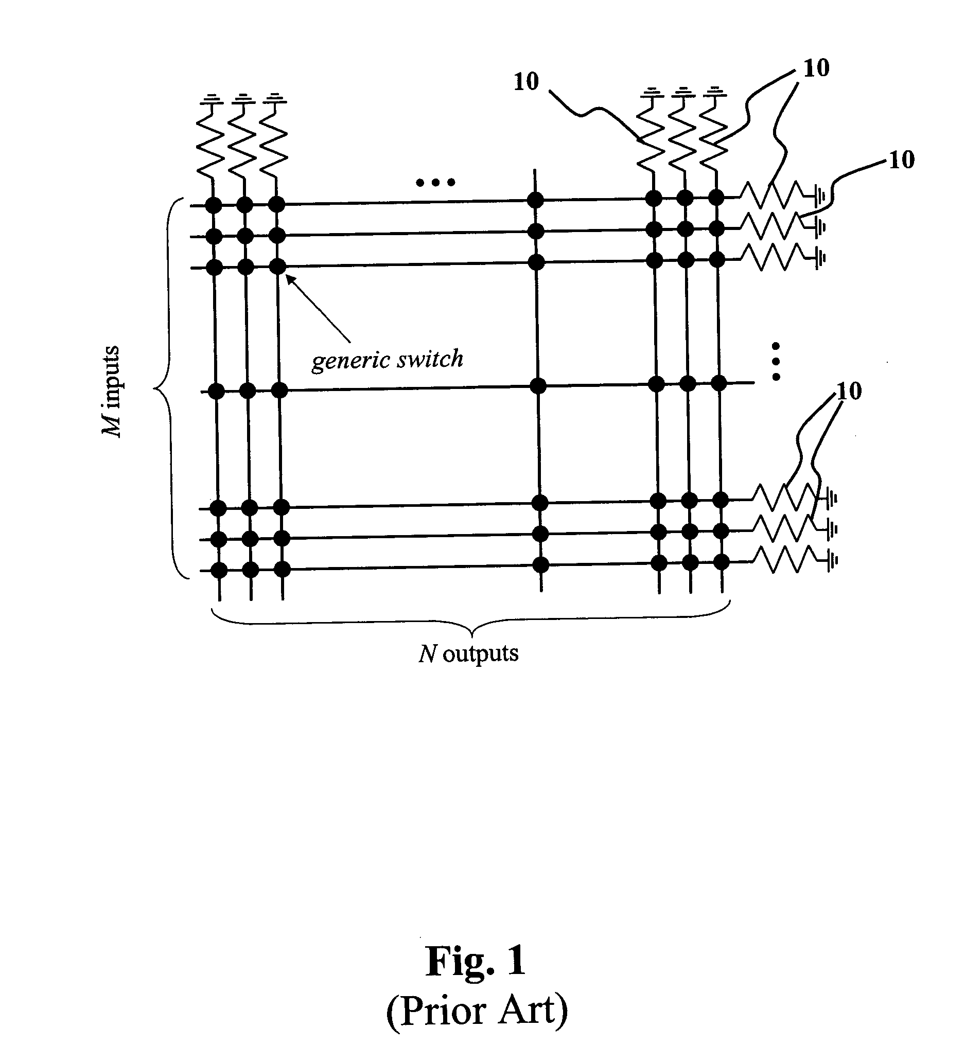
Provided that all of the lines have the same characteristic impedance and are terminated with the same impedance, this results in a minimum of 6 dB theoretical insertion loss for a high-frequency cross-point switch.
On the other hand, although 7–10 dB insertion loss per switch matrix may be manageable, cascading such matrix elements to achieve higher port count matrices can become troublesome without inserting intermediate amplifier stages to boost up the signal level.
Despite their advantages over conventional PIN diode switch matrices, GaAs latching PIN diode matrices have the following drawbacks: large circuit size, relatively high cost (i.e., low yield), difficulty in incorporating on-chip amplifiers, and difficulty in incorporating digital circuits.

Method used


Image

  • High speed cross-point switch using SiGe HBT technology
  • High speed cross-point switch using SiGe HBT technology
  • High speed cross-point switch using SiGe HBT technology

Examples


Embodiment Construction

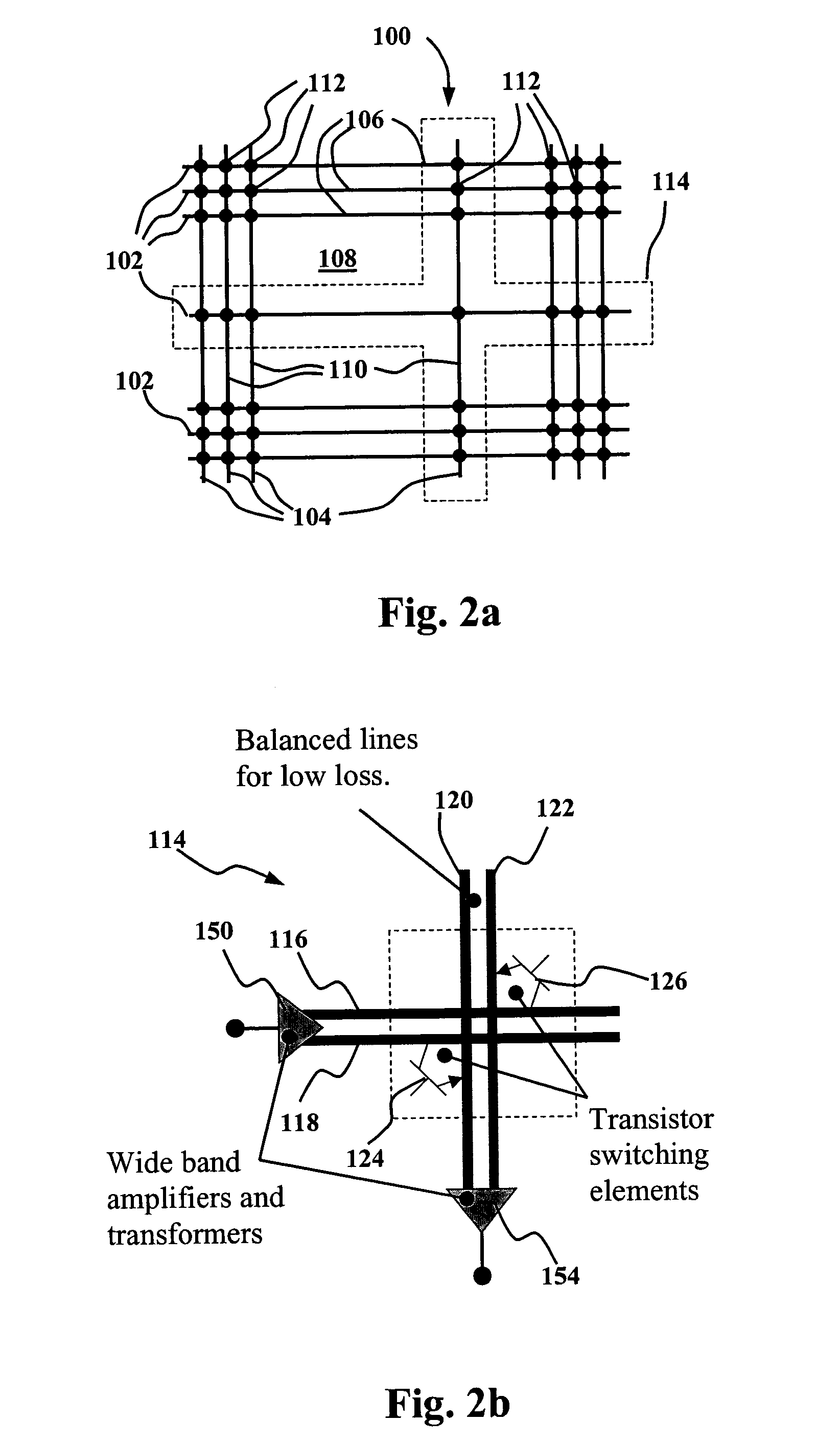
[0021]With reference to FIG. 2A, an M×N switch matrix indicated generally at 100 has M inputs (rows), 102, and N outputs (columns), 104. The M inputs, 102, introduce one or more signals to be switched onto a plurality of conductive microstrips, 106, which are arranged to extend in parallel in one direction over the face of a substrate, 108, such as a semiconductor substrate. A second set of conductive microstrips, 110, run in parallel over the face of the substrate, 108, at an angle to microstrips, 106, preferably at 90° thereto. A plurality of switching elements, 112, are formed at respective intersections of the input microstrips, 106, and the output microstrips, 110. These switching elements, 112, are selectively operated to connect ones of the inputs, 102, to ones of the outputs, 104, thereby being capable of switching signals input on the inputs, 102, to the outputs, 104, as desired.

[0022]The M×N switch matrix, 100, as shown in FIG. 2A is conceptual in that a single microstrip,...


PUM


Abstract

A high-speed cross-point switch is built on a preferably silicon substrate and uses bipolar transistor switching elements. Preferably, the bipolar transistors are SiGe bipolar junction transistors. Intersecting conductive input and output microstrips are preferably thinned at their intersections to reduce shunt capacitance between the coupled lines. It is also preferred that the input buffer be connected in cascode fashion with the switching transistors in order to create an amplification stage. The signal and its inverse are carried on balanced microstrip pairs in order to reduce electromagnetic field strength at the center of the balanced line pairs thereby improving isolation between two crossing balanced pairs.

Description

CROSS REFERENCE TO RELATED APPLICATIONS[0001]This application claims priority to U.S. provisional patent application Ser. No. 60 / 419,648 filed Oct. 18, 2002. The disclosure of that provisional patent application is fully incorporated by reference herein.FIELD OF THE INVENTION[0002]The present invention relates in general to high-speed cross-point switches, and more particularly to cross-point switches implemented using SiGe heterojunction bipolar transistors.BACKGROUND OF THE INVENTION[0003]Cross-point switches are commonly used in optical communication systems, test equipment, and transreceivers. Typical cross-point switch architecture is shown in FIG. 1. More particularly, high-frequency cross-point switches are commonly used in optical-millimeter wave-optical (OMO) switches. In OMO switches, the optical signal is first converted to a millimeter-wave (mm-wave) baseband signal. Then, switching is performed according to the requirements. Finally, the signal is converted to an optica...

Claims


Application Information

Patent Timeline
IPC IPC(8): H01L29/00H01P1/15H04L12/56
CPCH01P1/15H04L49/30H04L49/101H04L49/55
Inventor KINAYMAN, NOYAN
Owner COBHAM DEFENSE ELECTRONICS SYST CORP
Learn More