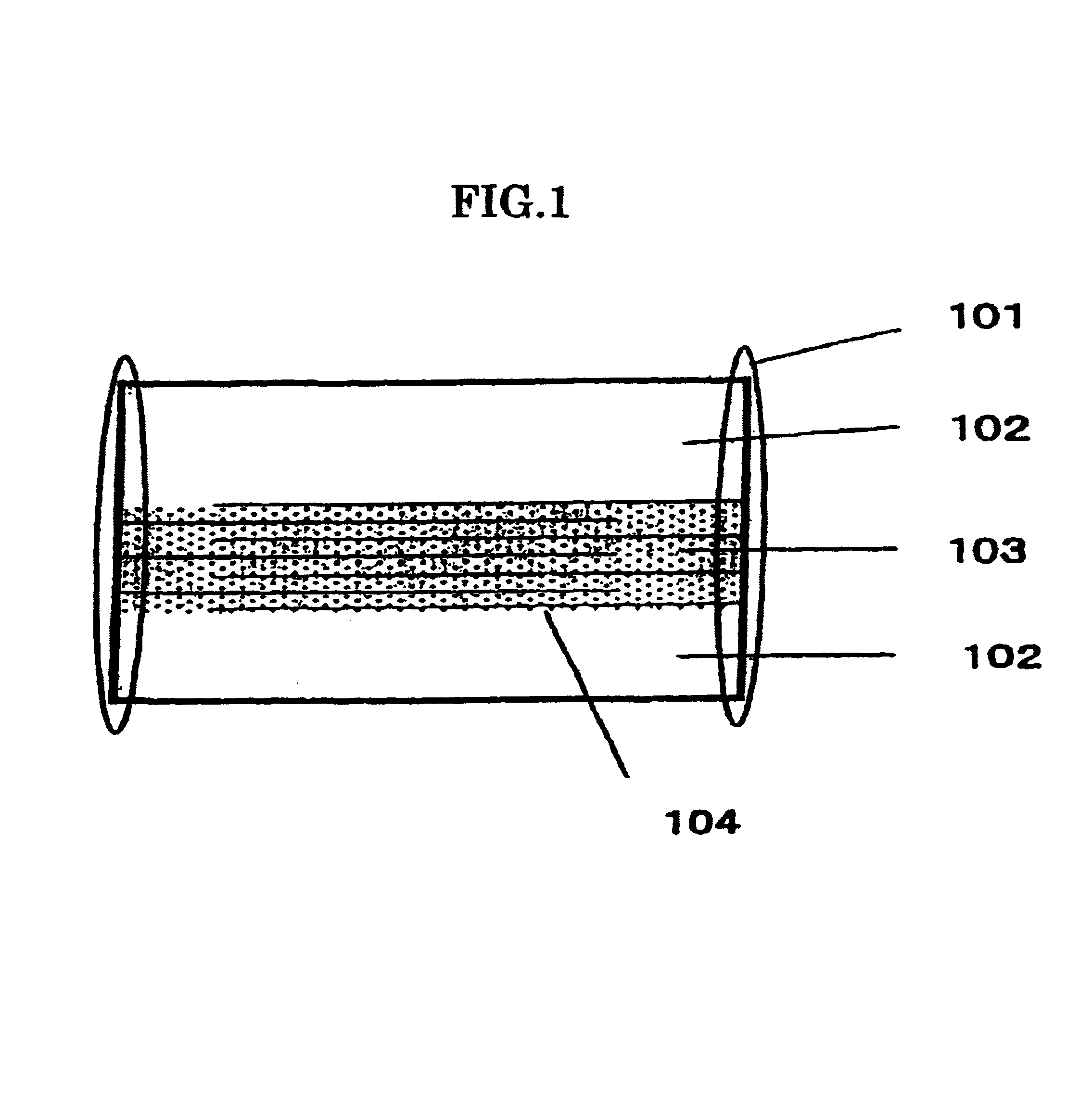
Conductive pattern incorporated in a multilayered substrate, multilayered substrate incorporating a conductive pattern, and a method of fabricating a multilayered substrate
a technology of multi-layered substrates and conductive patterns, which is applied in the direction of conductive pattern formation, fixed capacitor details, and other directions, can solve problems such as cracks, delaminations and the like, and increase conductor resistance, and increase the dielectric loss
- Summary
- Abstract
- Description
- Claims
- Application Information
AI Technical Summary
Benefits of technology
Problems solved by technology
Method used
Image


Examples
Embodiment Construction
Two types of glass-ceramic materials of different composition were prepared.
The first type (glass-ceramic A) consisted of glass composed of SiO.sub.2 : 62 mol %, Al.sub.2 O.sub.3 : 8 mol %, SrO: 20 mol %, CaO: 4 mol %, B.sub.2 O.sub.3 : 3 mol % and MgO: 3 mol %, and oxide aggregate composed of Al.sub.2 O.sub.3. The ratio of the oxide aggregate to the glass was 30:70 by volume. An organic vehicle including 15 parts by mass of acrylic resin as the binder, 50 parts by mass of toluene as the solvent, and 5 parts by mass of BPBG was added to and mixed with 100 parts by mass of the powder of the foregoing composition, and the result was processed into green sheets of 240 .mu.m thickness using the doctor blade method.
The second type (glass-ceramic B) consisted of glass whose composition was the same as the glass-ceramic A, and an oxide aggregate composed of Al.sub.2 O.sub.3 and TiO.sub.2 mixed at a ratio of 1:1 by volume. The ratio of the oxide aggregate to the glass was 30:70 by volume. T...
PUM
| Property | Measurement | Unit |
|---|---|---|
| temperature | aaaaa | aaaaa |
| melting point | aaaaa | aaaaa |
| mass % | aaaaa | aaaaa |
Abstract
Description
Claims
Application Information
 - R&D
- Intellectual Property
- Life Sciences
- Materials
- Tech Scout
- Unparalleled Data Quality
- Higher Quality Content
- 60% Fewer Hallucinations
Browse by: Latest US Patents, China's latest patents, Technical Efficacy Thesaurus, Application Domain, Technology Topic, Popular Technical Reports.
© 2025 PatSnap. All rights reserved.Legal|Privacy policy|Modern Slavery Act Transparency Statement|Sitemap|About US| Contact US: help@patsnap.com