
RF transition for an area array package

a technology of area array and transition, which is applied in the direction of semiconductor devices, semiconductor/solid-state device details, printed circuits, etc., can solve the problems of open-circuit failure by disconnection of signal lines, difficulty in mounting large ceramic bga packages on host printed circuit boards (pcbs) constructed using, and significant differences in the thermal expansion coefficient (cte) of most ceramic materials

Inactive Publication Date: 2005-05-10
VEONEER US LLC
View PDF17 Cites 34 Cited by
  • Summary
  • Abstract
  • Description
  • Claims
  • Application Information

AI Technical Summary

Problems solved by technology

The main problem with ceramic materials is that the coefficient of thermal expansion (CTE) of most of the ceramic materials is significantly different from the CTE of nearly all polymer and polymer-composite laminate printed circuit boards to which the package would be attached in a subsequent higher level assembly.
This poses a difficulty in mounting large ceramic BGA packages on host Printed Circuit Boards (PCBs) constructed using laminate materials, because standard size ball contacts nearly always develop cracks after thermal cycling unless additional precautions such as underfill are used.
These cracks eventually result in open-circuit failure by disconnection of the signal lines.
Finally, it is not easy to combine different ceramic materials having different dielectric constants into a functioning multilayer substrate, as would be desirable in the design of an RF or millimeter-wave package.
's technology is not suitable for packaging millimeter-wave circuits because using glob-top to cover the IC can deteriorate electrical performance due to the relatively high dielectric loss tangent of the glob-top materials.
In addition, the difference between the dielectric constants of the glob-top material and the substrate material that carries the transmission lines causes the isolation between the transmission lines to deteriorate.
However, Boutin et al., like Lan et al., only address the issue of encapsulating integrated circuits using transfer molding to prevent damage.
However, one of the disadvantages of this method is that it uses a thick film method to form the metal traces on the circuit, which has relatively low resolution compared to thin film and photolithographic techniques.
Another disadvantage is that during sintering, the circuitry shrinks.
Although the percentage of this shrinkage can be controlled precisely, the amount of shrinkage across the circuitry may not be constant if some parts of the circuitry contain more metals than other parts.
The disadvantage of Greenman's method is, as the package size becomes larger, the thermal expansion mismatch starts to be an issue.
Although pre-sintered ceramic materials provide a good solution from an electrical performance point of view for small packages at millimeter-wave frequencies, the thermal expansion mismatch problem makes them very difficult to use for larger package sizes.
It is known that the BGA transitions result in significant series inductance that deteriorates the reflection loss of the circuit at high frequencies.
This patent describes how to design broadband RF transitions for millimeter-wave IC packages though it does not address the actual packaging problems in detail.
Besides, coplanar waveguides are prone to excitation of higher order modes which can be an issue for electrically long transmission lines.
Another difficulty related to use of coplanar waveguides is that for the same impedance values and substrate heights, the width of the center conductor of the coplanar waveguides is narrow.
This increases the metallization losses and makes manufacturing more difficult.
However, in this patent, a thick-film technique is employed and due to the aforementioned difficulties, it is not suitable for large, high-density BGA millimeter-wave packages.

Method used


Image

  • RF transition for an area array package
  • RF transition for an area array package
  • RF transition for an area array package

Examples


Embodiment Construction

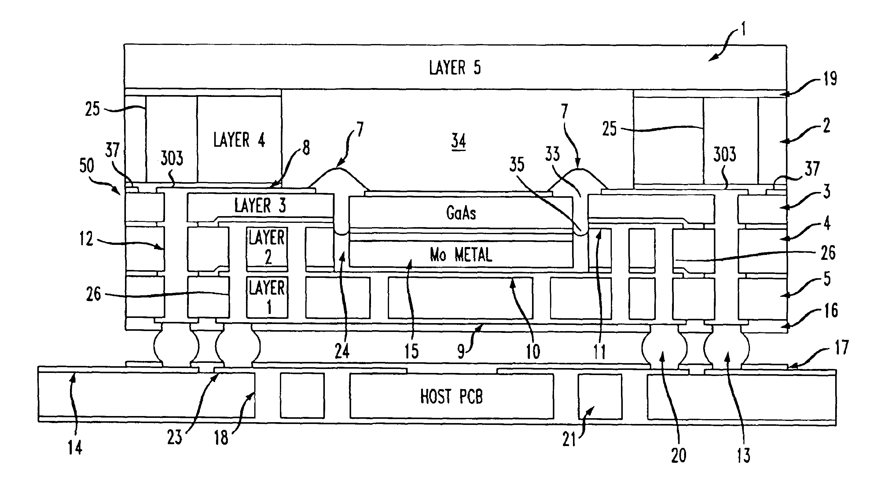
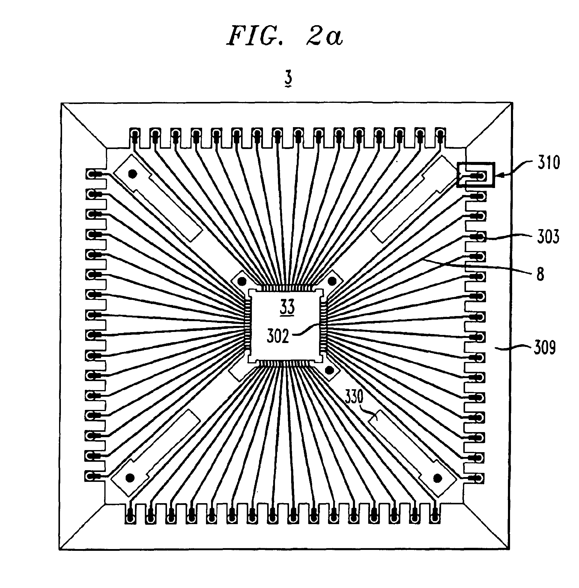
[0045]FIG. 1 shows the simplified cross-section of a PCB assembly 100, including a host PCB 21 and an exemplary multilayer package 50. In FIG. 1, horizontal distances are compressed and vertical distances are expanded for ease of understanding. The electrical connection between the package 50 and the host PCB 21 is achieved by using area array technology.

[0046]The monolithic microwave integrated circuit (MMIC) 6 is placed into the pockets 33 opened in the dielectric laminates 3 and 4. The exemplary package has five different construction layers 1-5. Top layer 1 may be made of an epoxy glass laminate, such as FR4 or similar material, or a stiff plastic, and is used to provide stiffness to the package, as well as to cover the internal IC assembly. This is important because top layer 1 reinforces the package planarity, which is required for a BGA type package 50.

[0047]Next, layer 2 is the superstrate layer. It has a rectangular opening 34 at the location where the MMIC 6 is going to be...


PUM


Abstract

A laminate multilayer ball-grid-array package is suitable for millimeter-wave circuits. The frequency bandwidth of the package is DC to 40 GHz. The package is made using laminate circuit board materials to match the temperature expansion coefficients of the package to the host PCB. Electrical connection between the package and the host PCB on which the package is mounted is achieved using ball-grid-array technology. The package can be sealed, covered, or encapsulated, and is suitable for high-volume production.

Description

FIELD OF THE INVENTION[0001]The present invention relates to semiconductor device packages generally, more specifically to area array packages, and more particularly to ball-grid-array (BGA) type packages that are used for RF and millimeter-wave integrated circuit (IC) packaging.BACKGROUND OF THE INVENTION[0002]Ball-grid-array (BGA) packages are commonly used in electronics to minimize circuit board area for a given circuit functionality. This is achieved by using the entire area under the package to create an array of I / O connections using pre-attached solder balls. BGA packages are also very suitable for high-volume production because automated pick-and-place machines can handle them and they are attached to the next higher level of assembly printed circuit board using solder re-flow methods.[0003]Ceramics are the materials most often used to build high-frequency BGA packages. Alumina, high-temperature co-fired (HTCC) ceramics, and low-temperature co-fired (LTCC) ceramics are exam...

Claims


Application Information

Patent Timeline
Patent Type & Authority Patents(United States)
IPC IPC(8): H01L23/02H01L23/58H01L23/055H01L23/66
CPCH01L23/055H01L24/32H01L23/66H05K1/0222H05K2201/09618H01L2224/16227H01L2224/32225H01L2224/48091H01L2224/48227H01L2224/73265H01L2924/01005H01L2924/01009H01L2924/01013H01L2924/01027H01L2924/01029H01L2924/01042H01L2924/01047H01L2924/01057H01L2924/01075H01L2924/01078H01L2924/01082H01L2924/09701H01L2924/14H01L2924/1423H01L2924/15153H01L2924/1517H01L2924/15173H01L2924/15311H01L2924/16195H01L2924/30105H01L2924/30107H01L2924/3011H05K1/0243H01L2924/01033H01L2924/01019H01L2924/01006H01L2224/16225H01L24/48H01L2924/00014H01L2924/00H01L2924/3512H01L2924/15787H01L2224/05599H01L2224/45099H01L2224/85399H01L2224/05573H01L2224/05568H01L2924/181H01L2224/2612H01L2224/45015H01L2924/207
Inventor KINAYMAN, NOYANZIEGNER, BERNARD A.ANDERSON, RICHARDLANTERI, JEAN-PIERREBUBER, M. TEKAMUL
Owner VEONEER US LLC
Learn More