
High numerical aperture objective lens manufacturable in wafer form

a technology of optical heads and objective lenses, which is applied in the field of manufacture and use of wafer-level optics with optical heads, can solve the problems of preventing the use of high-quality, high-number aperture lenses in the fabrication of high-quality, and the physical size of the head is rather bulky

Inactive Publication Date: 2000-04-11
SEAGATE TECH LLC
View PDF2 Cites 68 Cited by
  • Summary
  • Abstract
  • Description
  • Claims
  • Application Information

AI Technical Summary

Problems solved by technology

However, these processes are generally limited to a low-index glass (typically silica) with a spherical or near-spherical surface, or to a diffractive surface, preventing their use in the fabrication of high-quality, high numerical aperture lens.
Information storage technology and the storage capacity available therefrom has historically been limited by a number of factors.
Conventional magneto-optical heads tend to be based on relatively large optical assemblies which make the physical size of the head rather bulky.
Consequently, the speed at which conventional MO heads are mechanically moved to access new data tracks on a MO storage disk, known as a `seek time` is slow.
In addition, due to the large size of these optical assemblies, most commercially available MO disk drives use only one MO head to enable reads and writes to one side of a MO disk at a time.

Method used


Image

  • High numerical aperture objective lens manufacturable in wafer form
  • High numerical aperture objective lens manufacturable in wafer form
  • High numerical aperture objective lens manufacturable in wafer form

Examples


Embodiment Construction

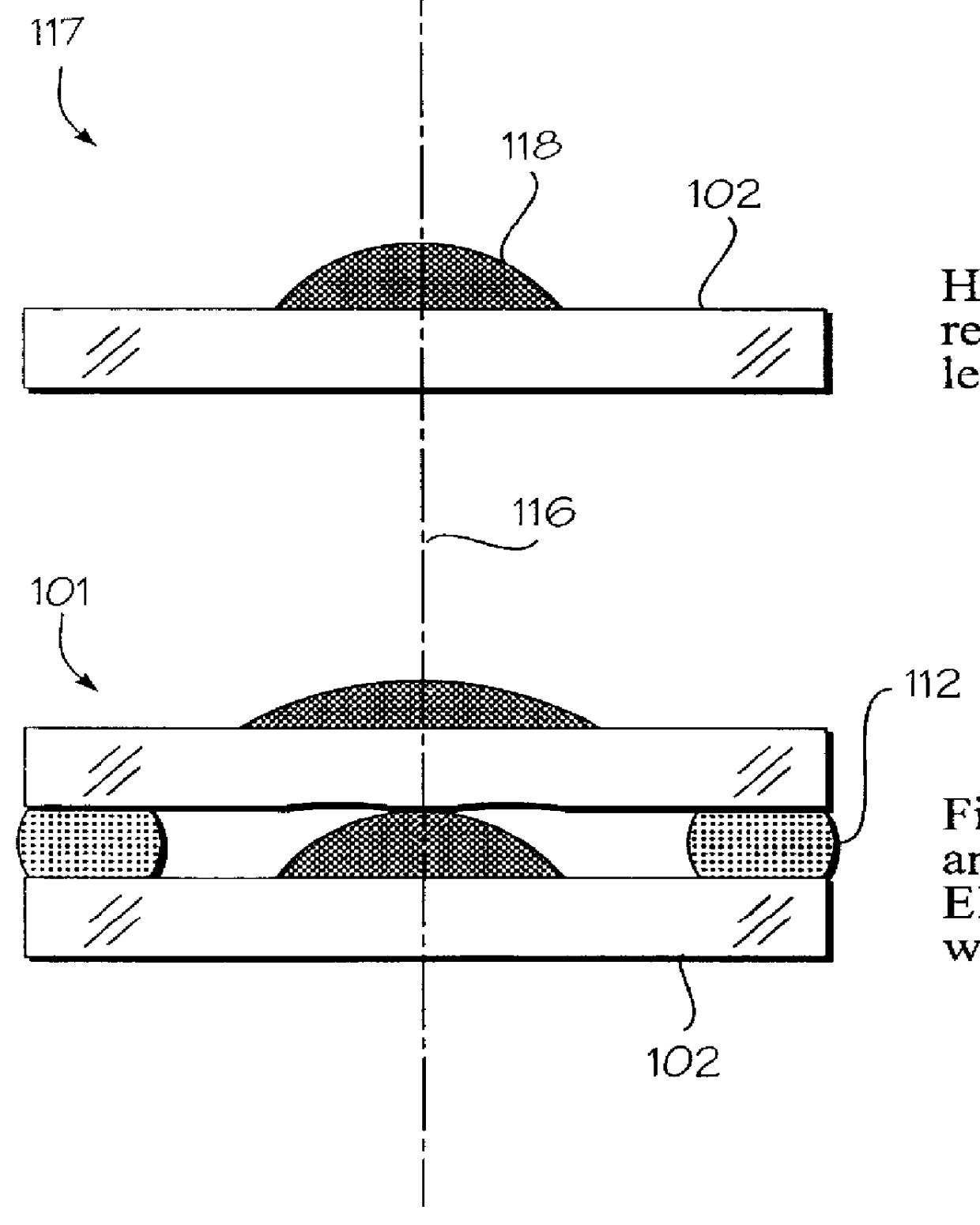
FIG. 1 is a cross-section view of a preferred embodiment assembly process for a composite micro-lens manufacture having two photoresist reflow lens elements;

FIG. 2 is an alternate embodiment of the composite micro-lens assembly combining a sphere and a photoresist reflow lens element;

FIG. 3 is the cross-section of the preferred embodiment;

FIG. 4 is the cross-section of the alternate embodiment;

FIG. 5 is a second alternate embodiment assembly process showing the sphere and a single piece lens-substrate element;

FIG. 6 is a 3D exploded view of a typical MO head showing the placement of the composite micro-lens; and

FIG. 7 is an expanded view of a 2D cross-section of a MO head, designed for wafer-level manufacture in an array.

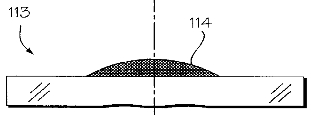
Referring to FIG. 1 there is seen a cross-section view depicting a set of basic assembly steps for a composite lens of a preferred embodiment. Here a first subassembly 113 is made using a wafer substrate 108 made from, for example, silica, which may be polished to a...


PUM


Abstract

A composite micro-lens for use in an optical or magneto-optical information storage system, made up of one or more lens elements which, when coupled in assembly, provide a desired numerical aperture. The design may provide, if necessary, a photo resist lens, a shaped ball lens, or one or more contoured surfaces within the composite construction to correct for aberrations. The composite lens designed in this manner allowing for the use of wafer-level assembly processes to provide high volume production capabilities. It is further intended that this micro-lens design support integration in an optical or magneto-optical head design.

Description

1. Field of the InventionThe present invention relates generally to manufacture and use of wafer level optics with optical heads and more particularly to manufacture and use of a high numerical aperture (NA) objective micro-lens through an assembly of subcomponents that can be produced in an array format using wafer-level techniques.2. Background ArtPrior to this invention, the manufacture of high numerical aperture objective lens involved a molding and a polishing of an aspheric surface using a high-index (of refraction) glass, techniques not capable of producing micro-lenses at high production rates. Current methods of producing a micro-part makes use of wafer-level processes, which can include an etch (ion milling), or a photoresist reflow technique. However, these processes are generally limited to a low-index glass (typically silica) with a spherical or near-spherical surface, or to a diffractive surface, preventing their use in the fabrication of high-quality, high numerical a...

Claims


Application Information

Patent Timeline
IPC IPC(8): G11B11/105G11B11/00G11B7/135
CPCG11B7/1374G11B7/1384G11B11/10543G11B2007/13727G11B11/10554G11B11/1058
Inventor HEANUE, JOHN F.WARDAS, MARK A.
Owner SEAGATE TECH LLC
Learn More