
Solution processible hardmasks for high resolution lithography

a technology of processible hardmasks and high resolution lithography, which is applied in the direction of liquid/solution decomposition chemical coating, instruments, photomechanical equipment, etc., can solve the problem that the thin resist layer does not have the etch budget to transfer patterns

Active Publication Date: 2012-09-06
INPRIA CORP
View PDF2 Cites 260 Cited by
  • Summary
  • Abstract
  • Description
  • Claims
  • Application Information

AI Technical Summary

Benefits of technology

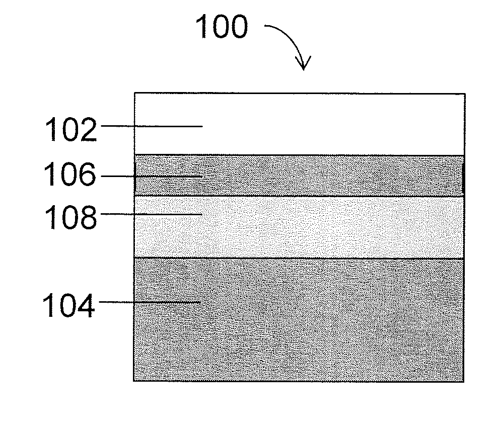
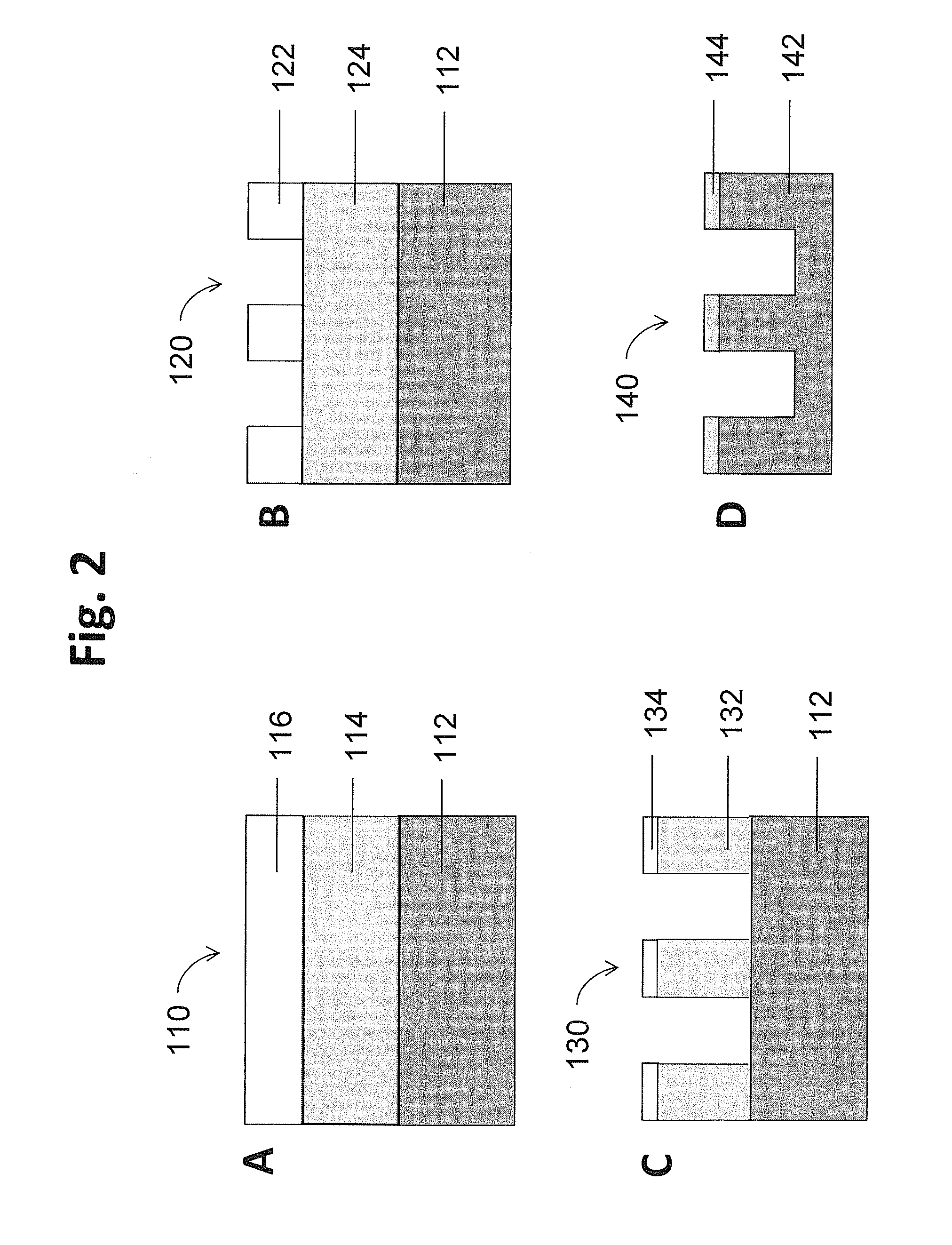
The invention is about a method for making a patterned structure on a layered structure that includes a substrate, a hardmask layer, and a resist layer. The method involves applying a hardmask precursor composition to the substrate, heating it to form a metal oxide hardmask layer, depositing a resist layer over the hardmask layer, and then exposing it to radiation to create the pattern. The invention also includes a layered structure that includes a substrate, a hardmask layer, and a resist layer, as well as a method for making this structure by heating an aqueous metal oxide precursor solution on a deposition surface to form a solid metal oxide layer and depositing a resist layer on top. The technical effects of this invention include improved precision and accuracy in patterning, as well as simplified and efficient processes for making the patterned structure.

Problems solved by technology

When combined with the limited etch selectivity between organic photoresists and functional materials, thin resist layers do not have the etch budget to transfer patterns directly into the functional device materials or the substrate.

Method used


Image

  • Solution processible hardmasks for high resolution lithography
  • Solution processible hardmasks for high resolution lithography
  • Solution processible hardmasks for high resolution lithography

Examples


example 1

Preparation of Metal Oxide Materials

[0132]This example describes a method that has been used to prepare metal oxide precursor solutions comprising polyoxometal clusters based on hafnium (Hf), zirconium (Zr), aluminum (Al), tungsten (W), and titanium (Ti).

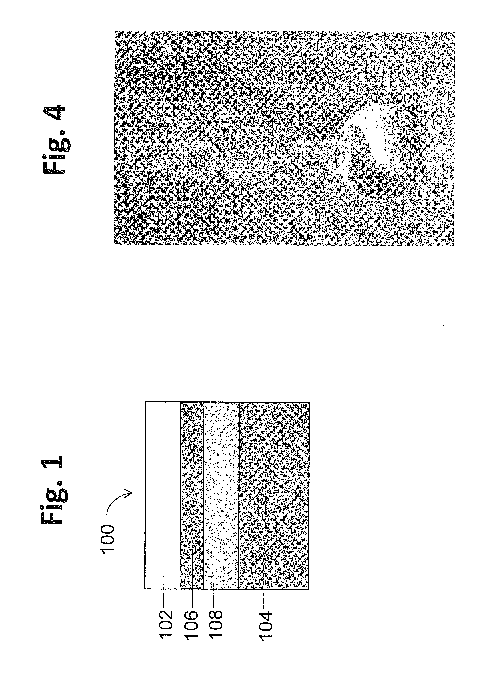
[0133]Metal-containing aqueous solutions were filtered and diluted before combining with diluted polyatomic anion solutions such as dilute H2SO4 solutions with optional addition of diluted H2O2 to form polyoxometal solutions with the concentration of specific components specified below. A photo of a representative metal oxide precursor solution is shown in FIG. 4, indicating the formation of a transparent clear solution.

[0134]AlOx(PO4)y: 0.56 M AlO+, 0.34 M PO42−;

[0135]HfOx(SO4)y: 0.4 M HfO+, about 0.26 M SO42−, and 1.2 M H2O2

[0136]Ti:ZrOx(SO4)y: 0.25 M TiO+, 0.25 M ZrO+, 1.5 M H2O2, and about 0.4 M SO42−

[0137]W:HfOx(SO4)y: 0.2 M HfO+, 0.04M WO42−, 0.6 M H2O2, and about 0.13 M SO42−

[0138]The polyoxometal solutions were then used to...

example 2

The Optical and Dielectric Properties of the Metal Oxide Hardmask

[0139]The optical and dielectric properties of the metal oxide materials formed in Example 1 were evaluated. Specifically, a precursor from the aluminum oxide phosphate AlOx(PO4)y family described in example 1 was spin-coated onto a Mo film to form a coating layer (also referred to as film) with a thickness of 110 nm. The aluminum oxide phosphate layer was cured at 350° C. although a process temperature in the range of 300 to 1000° C. can be used to make film or layer with a thickness of 2 were then formed by evaporating an array of Al dots onto the aluminum oxide phosphate layer. The optical properties of the film such as refractive index n and the extinction coefficient k of at different wavelength were extracted using a J.A. Woollam VASE ellipsometer and the results are shown in FIG. 5A. The dielectric properties of the film were extracted from MIM capacitor I-V / C-V data and shown in FIG. 5B. The optical and dielect...

example 3

Compatibility Studies of Metal Oxide Material on Various Substrate Surfaces

[0141]This example describes compatibility studies of the deposited materials on various substrate surfaces to determine the appropriate pre-treatment conditions to render the substrate surfaces hydrophilic and suitable for metal oxide coating. The polyoxometal precursors were made using the procedure outlined in Example 1.

[0142]Spin on carbon (SoC) hardmasks and silicon based anti-reflection coatings (Si-ARC) or layers on silicon wafers have been used as substrate surfaces. The Si-ARC and SoC materials are commercially available, and while used here for illustrative purposes, may not be representative of other materials with the same general function. The Si-ARC refers to a polymer containing Si with organic units or halide bound to the silicon, which are generally polysiloxanes. The Si-ARC coating on silicon wafer had a thickness of about 30 nm, comprises >30% silicon and was subjected to a 220° C., 60 s po...


PUM

PropertyMeasurementUnit
thicknessaaaaaaaaaa
thicknessaaaaaaaaaa
thickaaaaaaaaaa

Abstract

Solution processible hardmasks are described that can be formed from aqueous precursor solutions comprising polyoxometal clusters and anions, such as polyatomic anions. The solution processible metal oxide layers are generally placed under relatively thin etch resist layers to provide desired etch contrast with underlying substrates and / or antireflective properties. In some embodiments, the metal oxide hardmasks can be used along with an additional hardmask and / or antireflective layers. The metal oxide hardmasks can be etched with wet or dry etching. Desirable processing improvements can be obtained with the solution processible hardmasks.

Description

CROSS REFERENCE TO RELATED APPLICATIONS[0001]This application claims priority to copending U.S. provisional patent application 61 / 447,477 to Stowers et al. filed on Feb. 28, 2011, entitled “Solution Processable Inorganic Hardmask,” incorporated herein by reference.STATEMENT AS TO GOVERNMENT RIGHTS[0002]Development of the inventions described herein was at least partially funded with government support through U.S. National Science Foundation grants DGE-0549503 and IIP-0912921, and the U.S. government has certain rights in the inventions.FIELD OF THE INVENTION[0003]The invention relates to structures with an inorganic hardmask layer comprising metal oxides for patterning inorganic substrates with micron or submicron resolution as well as to the corresponding patterned structure. The substrates can comprise silicon or other semiconductor materials for the formation of integrated circuits or the like. The invention further relates to methods for forming an inorganic hardmask layer usin...

Claims


Application Information

Patent Timeline
Patent Type & Authority Applications(United States)
IPC IPC(8): H01L23/00H01L21/311
CPCC23C18/06C23C18/1216H01L21/02178H01L21/02181H01L21/02189H01L21/02194G03F7/16H01L21/0332H01L21/3081H01L21/31122G03F7/091G03F7/094H01L21/02282H01L21/31641H01L21/0338H01L21/3088
Inventor STOWERS, JASON K.MEYERS, STEPHEN T.KOCSIS, MICHAELKESZLER, DOUGLAS A.GRENVILLE, ANDREW
Owner INPRIA CORP
Learn More