
Method for producing a resistive heating element

a heating element and resistive technology, applied in the direction of resistors, non-adjustable resistors, carbon-silicon compound conductors, etc., can solve the problems of high precision, time and expense, and difficulty in mechanical processing of flat conducting layers, so as to achieve narrow tolerances, large tolerances, and large tolerances

Inactive Publication Date: 2005-05-10
CVT
View PDF5 Cites 2 Cited by
  • Summary
  • Abstract
  • Description
  • Claims
  • Application Information

AI Technical Summary

Benefits of technology

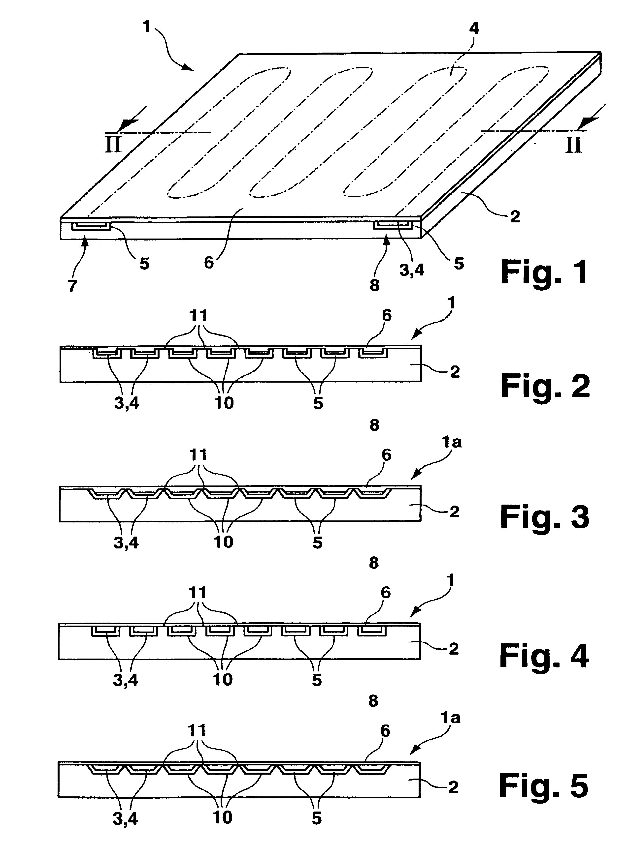
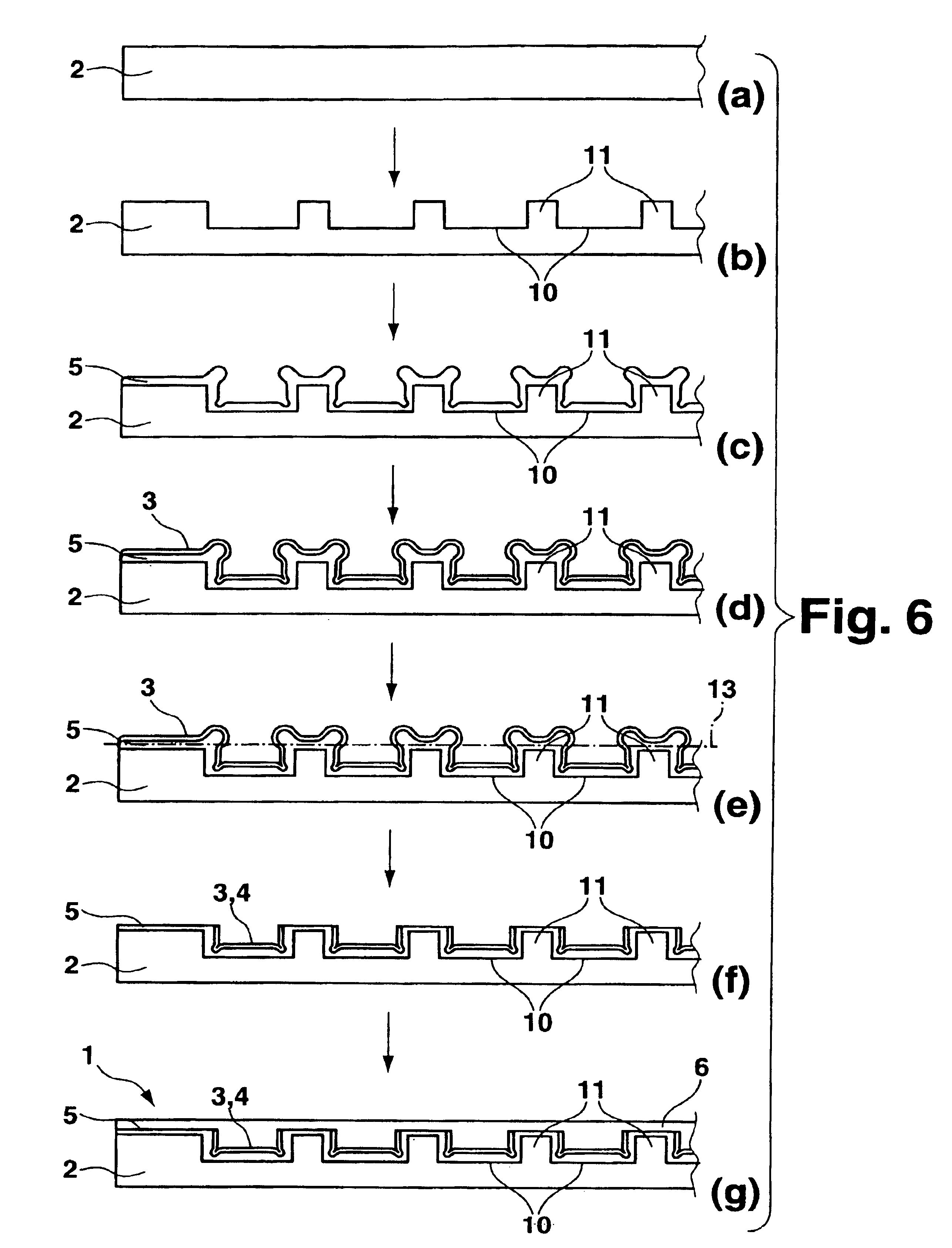
[0007]In accordance with the invention, the substrate is mechanically prepared in correspondence with the desired shape of the conductor path to produce a recess which receives the conductor path, subsequently deposited from the gaseous phase. Mechanical preparation may be performed using any machining method, such as milling, grinding or the like and requires only relatively large tolerances. The layer of insulating material is then deposited onto the mechanically prepared substrate followed by gaseous phase deposition of the layer of conducting material, wherein the layer thickness of the insulating material may be relatively low, e.g. approximately 0.5 mm or less. The thickness of the layer of conducting material depends on the desired electrical resistance of the resistive heating element. After application of the two layers, at least the external layer of conducting material is evenly removed until the conducting material has been completely removed at least in the raised regions of the substrate bordering the recess of the conductor path thereby forming the conductor path, wherein the insulating layer disposed below the conducting layer becomes visible at the raised regions of the substrate to completely separate the individual conductor paths from each other through interposition of the insulating material. This can be produced through large-surface grinding. If the depth of the recess in the substrate is sufficient, the conducting layer can be removed in a rapid and straightforward fashion, thereby requiring relatively large tolerances in the region of 0.1 mm. Due to the initial formation of the recess in the substrate and deposition of the insulating layer and the conducting layer onto the surface contour formed in this fashion, the conductor path is consequently produced through planar removal of the conducting layer from the raised regions of the substrate which border the recess. This procedure is much simpler than the process of prior art with which the conductor path must be cut out of the evenly deposited conducting layer thereby keeping very narrow tolerances without locally destroying the underlying insulation layer.
[0008]In a preferred embodiment, the raised regions bordering the conductor path have sharp edges caused by machining of the substrate, wherein the raised regions of the substrate can be e.g. substantially square and / or saw-tooth shaped. Advantageously, deposition is thereby increased in the edge regions of the substrate between the recess and the raised regions during coating of the substrate via chemical vapor deposition. The increased thickness of the insulating layer in the edge regions ensures insulation on all sides of the formed conductor path during subsequent planar removal of the conducting layer.
[0009]Various materials can be principally used as the substrate carrier material, having material properties suitable for the respective purpose of use. Preferably, a substrate of graphite is used which is inexpensive and has a high rigidity and temperature resistance.
[0010]While pyrolytic boron nitride (PBN) is preferably used as the electrically insulating layer, pyrolytic carbon (pyrocarbon, PC) is preferably disposed as the electrically conducting layer. The mentioned materials have excellent insulating and conducting properties and can be easily deposited from the gaseous phase. They also have a high temperature stability. Boron nitride (white) has a different color than carbon (black) such that when the conducting layer is evenly removed, they can be easily visually distinguished and the pyrocarbon layer can be removed e.g. in a level fashion until the underlying boron nitride layer shows at the raised regions of the substrate to ensure insulation of the conductor path at all sides.
[0015]The invention also concerns a resistive heating element having a substrate on which an electrically insulating layer is deposited, onto which an electrically conducting layer is deposited in the form of at least one conductor path which is, in particular, produced using a method of the above-mentioned type. In accordance with the invention, the conductor path is embedded in at least one recess of the substrate which is defined and bordered by raised regions formed in the substrate. The raised regions which define and limit the recess with the conductor path, insulate the sides of the conductor path and permit simple and inexpensive production of the resistive heating element through even removal of the conducting layer deposited on the surface contour of the substrate, thereby interposing the insulating layer.

Problems solved by technology

The mechanical processing of the flat conducting layer requires an excessive amount of time and expense and, in particular, requires high precision with tolerances of better than 0.01 mm, since short-circuits in the generated conductor path must be prevented and therefore the layer of conducting material between the regions which form the conductor path and which remain on the insulating layer must be completely removed.
This renders processing more difficult.

Method used


Image

  • Method for producing a resistive heating element
  • Method for producing a resistive heating element
  • Method for producing a resistive heating element

Examples


Embodiment Construction

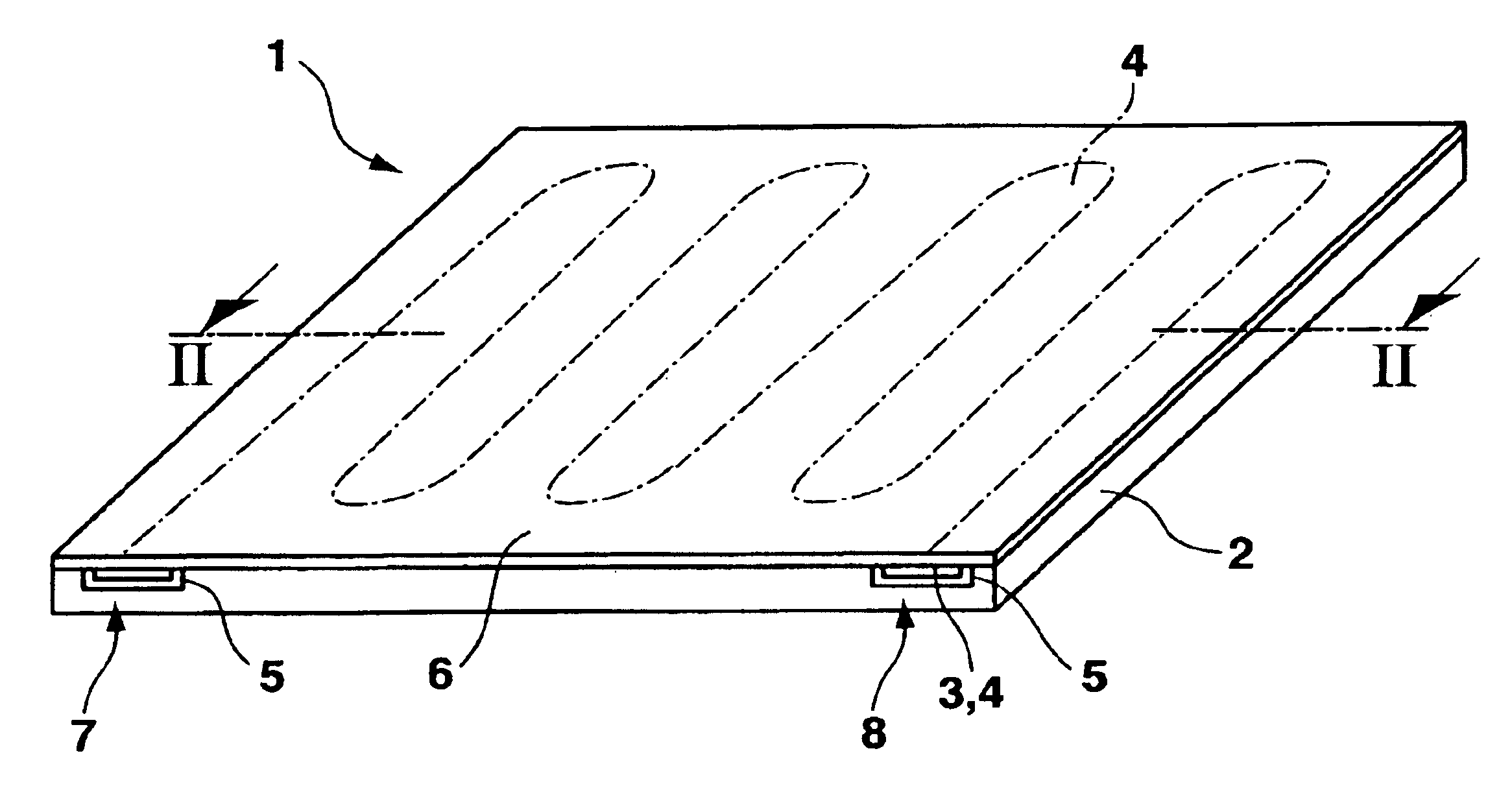
[0027]FIG. 1 shows an embodiment of an inventive resistive heating element 1. The resistive heating element 1 comprises a substrate 2 which serves as carrier material and which is substantially plate-shaped, e.g. of graphite, and an electrically conducting layer 3 in the form of a, in the present embodiment, meandering conductor path 4 (shown with dash-dotted lines) e.g. of pyrolytic carbon. An insulating layer 5, e.g. of pyrolytic boron nitride is disposed between the substrate 2 and the conducting layer 3 forming the conductor path 4. Moreover, the side of the conducting layer 3 facing away from the substrate 2 is provided with an insulating covering layer 6 for protecting the conductor path 4 from external effects which also consists e.g. of pyrolytic boron nitride. The ends of the conductor path 4 connecting to an outer side of the resistive heating element 1 serve as terminals 7, 8 for applying an electric voltage.

[0028]As shown in FIG. 2, the conductor path 4 is embedded in a ...


PUM

PropertyMeasurementUnit
thicknessaaaaaaaaaa
temperaturesaaaaaaaaaa
electrically insulatingaaaaaaaaaa

Abstract

Method for producing a resistive heating element by coating a substrate with an electrically insulating material from the gaseous phase, depositing an electrically conducting material from the gaseous phase onto the layer of insulating material deposited onto the substrate, wherein the layer of conducting material deposited onto the layer of insulating material is subsequently partially mechanically removed thereby forming at least one conductor path. The substrate is machined before depositing the insulating material thereby forming at least one recess provided for receiving the conductor path. The layers of insulating material and conducting material are deposited onto the mechanically processed substrate. Finally, the layer of conducting material is evenly removed until at least the conducting material has been completely removed from the elevated regions of the substrate delimiting the recess of the conductor path, thereby forming the conductor path. The invention also concerns a resistive heating element produced in this fashion.

Description

[0001]This application claims Paris Convention priority of DE 102 09 080.7 filed Mar. 01, 2002 the complete disclosure of which is hereby incorporated by reference.BACKGROUND OF THE INVENTION[0002]The invention concerns a method for producing a resistive heating element by coating a substrate with an electrically insulating material from the gaseous phase, depositing an electrically conducting material from the gaseous phase onto the layer of insulating material deposited onto the substrate, and subsequent mechanical removal of at least parts of the layer of a conductive material deposited onto the layer of insulating material thereby forming at least one conductor path. The invention also concerns a resistive heating element comprising a substrate onto which an electrically insulating layer is disposed, with an electrically conducting layer in the form of at least one conductor path being disposed onto the insulating layer.[0003]Resistive heating elements of this type are conventio...

Claims


Application Information

Patent Timeline
Patent Type & Authority Patents(United States)
IPC IPC(8): H01B1/04H01C17/075H01C7/00H01C17/08H01B3/12C04B41/52C04B41/89
CPCC04B41/009C04B41/89H01B1/04H01B3/12H01C7/008H01C17/08C04B41/52C04B41/4529C04B41/4572C04B41/5064C04B41/4527C04B41/522C04B41/4576C04B41/5001C04B35/522Y10T29/49087C04B2111/00844Y10T29/49155Y10T29/49144Y10T29/49085Y10T29/49083
Inventor GOETZ, ULRICH
Owner CVT
Learn More