
Pre-anneal of CoSi, to prevent formation of amorphous layer between Ti-O-N and CoSi

a technology of cosi and ti-o-n, which is applied in the direction of semiconductor devices, semiconductor/solid-state device details, electrical apparatus, etc., can solve the problems of forming devices having a titanium oxynitride diffusion barrier atop a cobalt silicide, and electrically open circuit,

Inactive Publication Date: 2005-04-12
GLOBALFOUNDRIES INC
View PDF6 Cites 20 Cited by
  • Summary
  • Abstract
  • Description
  • Claims
  • Application Information

AI Technical Summary

Benefits of technology

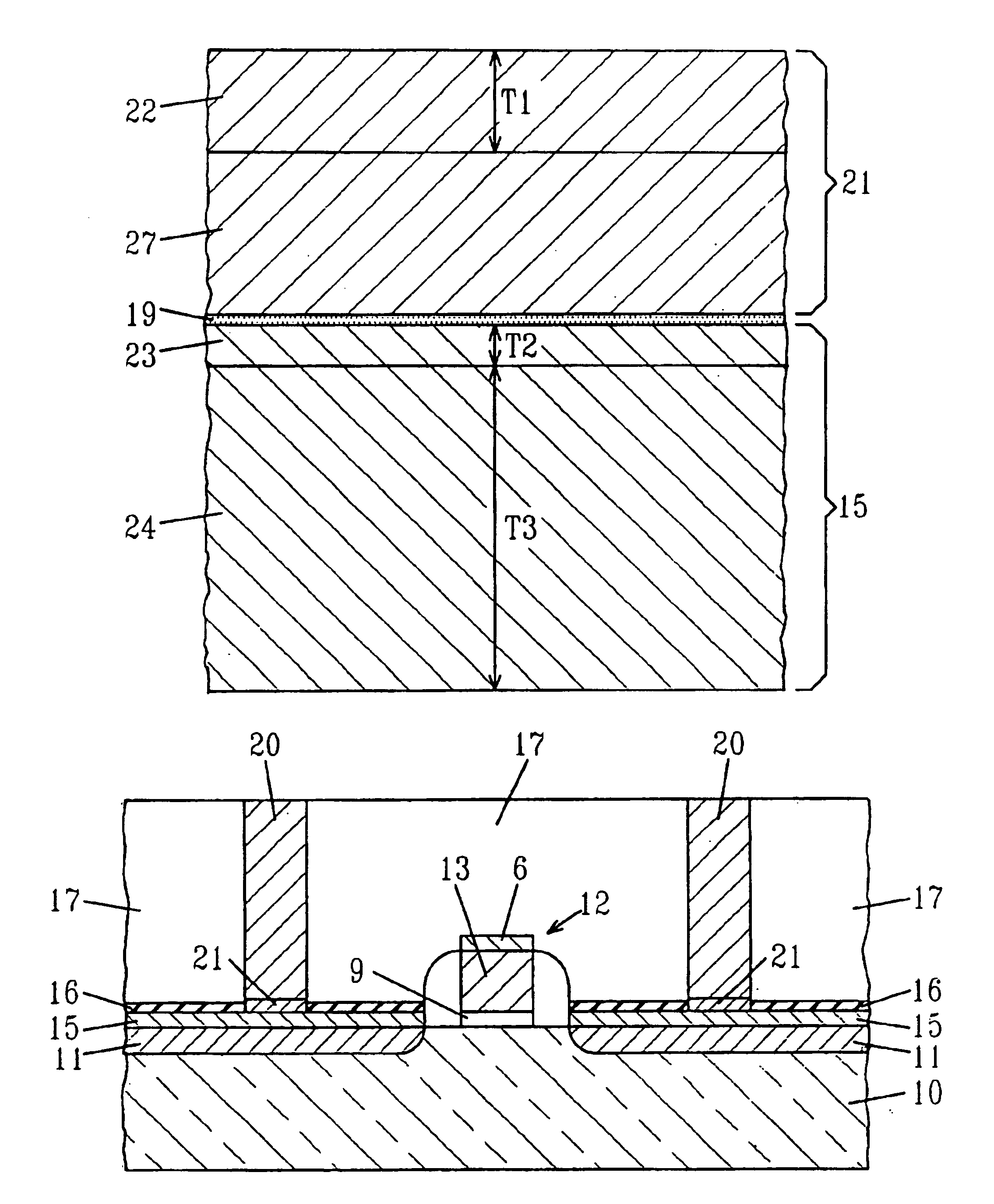
The present invention provides methods for forming a via interconnect to a silicide region comprising cobalt or nickel, with an effective barrier layer comprising a Group IVA metal nitride, such as titanium nitride or zirconium nitride, between the silicide and the metal layer. The methods involve depositing a Group IVA metal layer atop a nitrogen passivation layer formed on the silicide, and annealing the layers in a nitrogen-containing ambient to form the diffusion barrier. The nitrogen passivation layer prevents the diffusion of metals from the Group IVA metal layer. The methods also involve depositing an interconnect metal within the vias and atop the metal nitride diffusion barrier. The invention provides a thinner amorphous Group IVA metal silicide layer and a thicker metal nitride diffusion barrier layer, which maintains the effectiveness of the barrier layer during chemical vapor deposition of tungsten from tungsten hexaflouride.

Problems solved by technology

Forming devices having a titanium oxynitride diffusion barrier atop a cobalt silicide has presented difficulty when processed with corresponding tungsten vias.
If the titanium nitride diffusion barrier layer is too thin to be an effective barrier to fluorine, the fluorine may attack the underlying amorphous titanium cobalt silicide layer resulting in a ruptured via producing an electrically open circuit.

Method used


Image

  • Pre-anneal of CoSi, to prevent formation of amorphous layer between Ti-O-N and CoSi
  • Pre-anneal of CoSi, to prevent formation of amorphous layer between Ti-O-N and CoSi
  • Pre-anneal of CoSi, to prevent formation of amorphous layer between Ti-O-N and CoSi

Examples


Embodiment Construction

The inventive method for forming a low resistance via will now be discussed in greater detail referring to the drawings accompanying the present invention. It is noted in the accompanying drawings like and corresponding elements are referred to by like reference numbers.

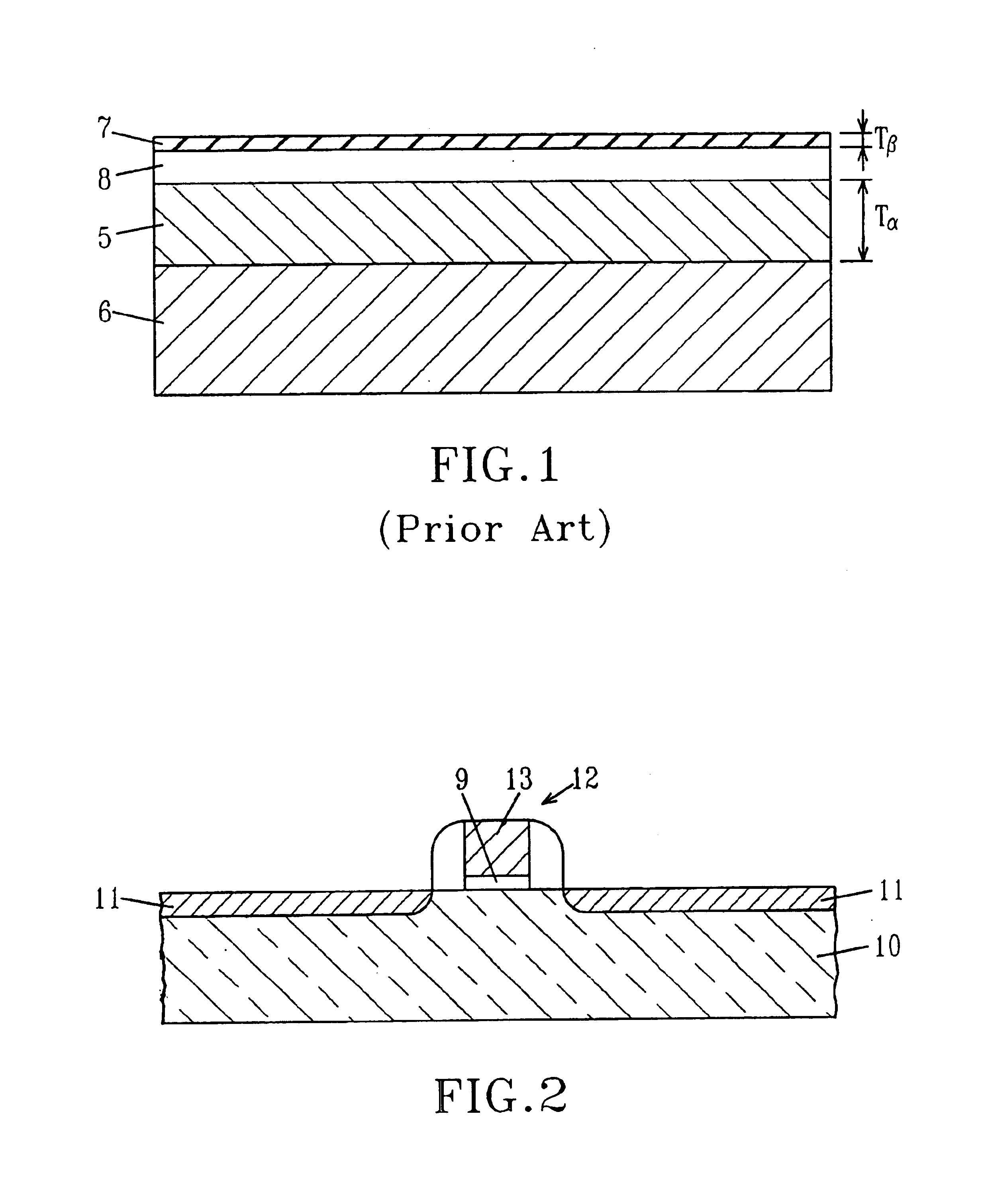
Referring to FIG. 2, a substrate 10 of silicon-containing material is first provided. Silicon-containing materials include, but are not limited to: silicon, single crystal silicon, polycrystalline silicon, silicon germanium, silicon-on-silicon germanium, amorphous silicon, silicon-on-insulator (SOI), silicon germanium-on-insulator (SGOI), and annealed polysilicon. The substrate may further comprise the source / drain regions 11 and gate region 12 of a complementary metal oxide semiconducting device. The gate region 12 may include a gate dielectric 9 and polysilicon gate conductor 13.

Referring to FIG. 3, a silicide region 15 is then formed atop the source and drain regions 11. A gate silicide region 6 also forms atop th...


PUM

PropertyMeasurementUnit
temperatureaaaaaaaaaa
thicknessaaaaaaaaaa
temperatureaaaaaaaaaa

Abstract

The present invention provides a method for forming an interconnect to a cobalt or nickel silicide having a TiN diffusion barrier. The inventive method comprises providing an initial structure having vias to exposed silicide regions positioned on a substrate; annealing the initial structure in a nitrogen-containing ambient, wherein a nitrogen passivation layer is formed atop the exposed silicide region; depositing Ti atop the nitrogen passivation layer; annealing the Ti in a nitrogen-containing ambient to form a TiN diffusion barrier and an amorphous Ti cobalt silicide between the TiN diffusion layer and the cobalt or nickel silicide and depositing an interconnect metal within the vias and atop the TiN diffusion barrier. The nitrogen passivation layer substantially restricts diffusion between the Ti and silicide layers minimizing the amorphous Ti cobalt silicide layer that forms. Therefore, the amorphous Ti cobalt or Ti nickel silicide is restricted to a thickness of less than about 3.0 nm.

Description

FIELD OF INVENTIONThe present invention relates to semiconductor devices and a method of manufacture, more particularly to an improved via interconnect to a silicide region.BACKGROUND OF THE INVENTIONBarrier layers and silicide layers are often an integral part of semiconducting devices. Materials which function as barriers to metal diffusion may be incorporated in metal interconnect structures that are part of integrated circuits (ICs). Barriers to metal diffusion are typically required to generate reliable devices, since low-k interlayer dielectrics typically do not prohibit metal diffusion.Silicide contacts are of specific importance to IC's, including complementary metal oxide semiconductor (CMOS) devices because of the need to reduce the electrical resistance of the many Si contacts, at the source / drain and gate regions, in order to increase chip performance. Silicides are metal-silicon compounds that are thermally stable and provide for low electrical resistivity at the Si / met...

Claims


Application Information

Patent Timeline
Patent Type & Authority Patents(United States)
IPC IPC(8): H01L23/52H01L21/44H01L21/02H01L21/336H01L21/768
CPCH01L21/28518H01L21/76814H01L29/665H01L21/76855H01L21/76856H01L21/76843H01L23/485
Inventor BRULEY, JOHNCABRAL, JR., CYRILLAVOIE, CHRISTIANWAGNER, TINA J.WANG, YUN YUWILDMAN, HORATI S.HON, WONG KWONG
Owner GLOBALFOUNDRIES INC
Learn More