Compact ATE with time stamp system

a time stamp and compact technology, applied in the field of automatic test equipment, can solve the problems of limited resolution, inadequacy, and inability to distinguish, and achieve the effect of low cos

Inactive Publication Date: 2005-03-15
TERADYNE
View PDF9 Cites 40 Cited by
  • Summary
  • Abstract
  • Description
  • Claims
  • Application Information

AI Technical Summary

Benefits of technology

Also, as a particular problem for ATE, we have recognized that use of ECL components for time measurement reduces the level of integration of the overall test system. Much of a test system is built with CMOS circuitry. CMOS circuitry is small, allowing for high levels of integration on a chip. ECL circuits are built using different processes than CMOS and will likely be on a separate chip. The extra chip, as well as the added space consumed by including I / O pads in the CMOS chips to connect to the ECL chip increases cost and reduces the level of integration of the overall test system. These problems are magnified in ATE because ATE generally consists of hundreds and sometimes thousands of channels in which separate signals are generated. Therefore, numerous copies of the chips will be required in each ATE system.
An alternate approach to a timestamp is to have two delay lines, one of which delays the clock and the other delaying the edge being measured. The delay elements on the clock path have delay T1 and the delay elements on the edge input have delay T2. At each delay stage, the clock path outputs are tied to the clock input of a latch and the edge path outputs are tied to the D input of the latch. Then each stage in the delay path can be used to measure a time difference of T2-T1 compared to the previous stage. Such a circuit is easily implemented in CMOS as is described in C. Tommas Gray, Willhelmus A. M. Van Nojije and R. K. Cavin “A sampling Technique and Its CMOS Implementation with 1 Gb / s Bandwidth and 25 ps Resolution”, IEEE J. Solid-state Circuits, vol.29. No.3. pp.340-349, Mar. 1994. However, the delay through the full delay line is T1*Tclk / (T2-T1), or for example 16 times the clock period Tclk if T2-T1 is {fraction (1 / 16)} of T1. This means the refire time (time before the timestamp can be reused) is long, at least 16 clock cycles, and the signal accumulates errors due to jitter and power supply noise during this entire time period.
Both of these methods can be implemented with a standard CMOS process. In the delay line method, a higher resolution is obtained by utilizing more buffers so that the delay of each buffer is smaller. In the vernier method, the minimum time that can be measured is set up by buffer delay difference in the two DLL lines. However, greater resolution is achieved with longer delay lines, too. A delay locked loop is used to stabilize the value of buffer delay against process variation and ambient condition. However, long delay lines have the undesired effect of creating a long re-fire time. And, long delay lines also make the noise jitter worse along the line. The measurement accuracy must be downgraded because of the jitter. For example, in a 400 Mhz clock system we need two N=256 delay stages line to achieve 10 ps timing resolution. A further drawback of making a high resolution time measurement circuit is that the long delay line draws a lot of current, which can make it unsuitable for use in a highly integrated system, such as a test system. For example, an article entitled “A High-resolution CMOS Time-to-digital Converter Utilizing a Vernier Delay Line,” IEEE JSSC, vol.25, no.2, Feb. 2000, describes a 35 ps time resolution time measurement system using two 128-delay stage lines.
With the foregoing background in mind, it is an object to provide a low cost, compact time stamp system.

Problems solved by technology

Thus, to measure the timing of these signals, it is not adequate for ATE to generate edges relative to a master clock.
The drawback of a simple counter is that it has limited resolution.
However, there is no way to distinguish between signals that happen early in that window or late in the window, so the resolution of the measurement is limited by the period of the clock.
Often, time measurement with a resolution limited by the period of the clock will not be adequate.
A drawback of this approach is that the interpolator must be made with very stable circuitry.
Variations in the delays introduced by the interpolator limit the accuracy of the measurements.
For example, variations in delay can be caused by changes in operating temperature or other environmental factors.
However, ECL components are expensive and not widely available.
Also, as a particular problem for ATE, we have recognized that use of ECL components for time measurement reduces the level of integration of the overall test system.
The extra chip, as well as the added space consumed by including I / O pads in the CMOS chips to connect to the ECL chip increases cost and reduces the level of integration of the overall test system.
These problems are magnified in ATE because ATE generally consists of hundreds and sometimes thousands of channels in which separate signals are generated.
Further, ECL components consume relatively large amounts of power in comparison to CMOS.
High power consumption is a drawback for circuitry in ATE.
However, if these circuits consume large amounts of power, they also generate large amounts of heat.
Packing such chips close together results in a high heat density, which in turn creates a need for complicated cooling systems.
Thus, using chips with higher power utilization has side effects that further increase the cost, size and complexity of ATE.
This means the refire time (time before the timestamp can be reused) is long, at least 16 clock cycles, and the signal accumulates errors due to jitter and power supply noise during this entire time period.
However, long delay lines have the undesired effect of creating a long re-fire time.
And, long delay lines also make the noise jitter worse along the line.
A further drawback of making a high resolution time measurement circuit is that the long delay line draws a lot of current, which can make it unsuitable for use in a highly integrated system, such as a test system.
However, that patent does not describe a time stamp incorporated into ATE.

Method used


Image

  • Compact ATE with time stamp system
  • Compact ATE with time stamp system
  • Compact ATE with time stamp system

Examples


Embodiment Construction

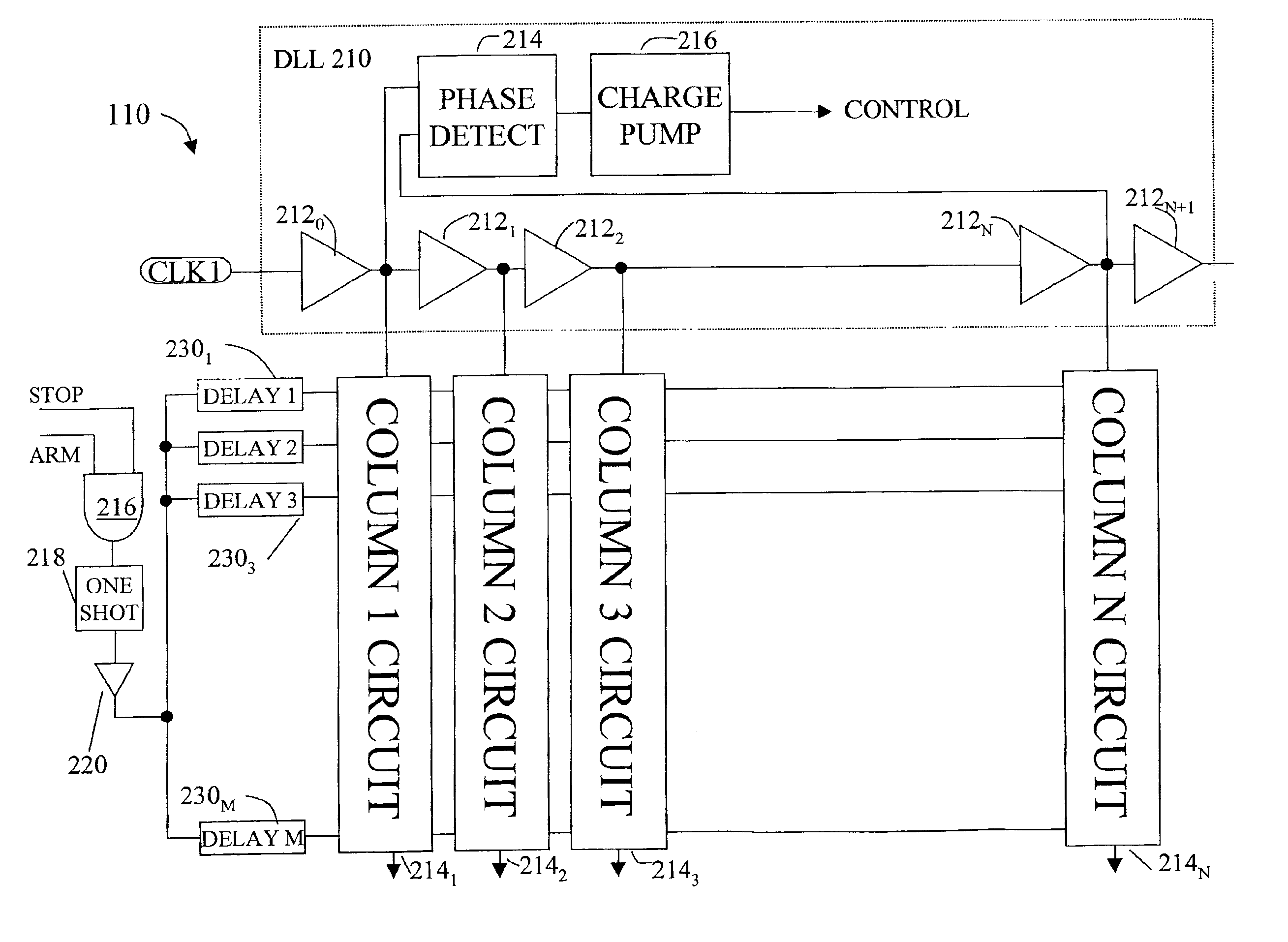
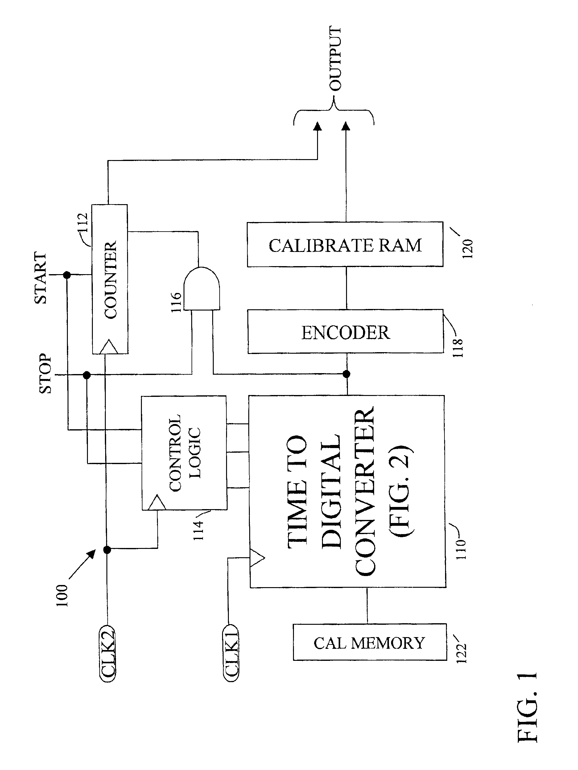
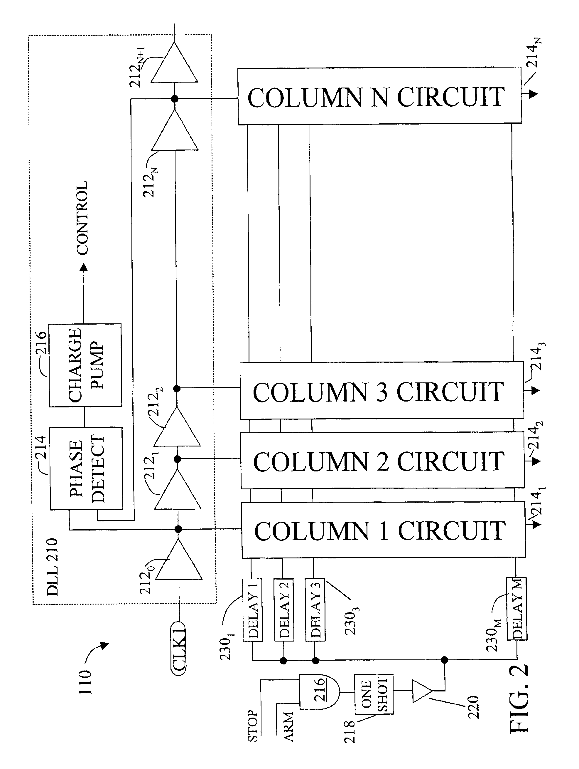
FIG. 1 shows a time stamp system incorporating the invention. A START and STOP signal are applied to the system and the system produces a digital OUTPUT that reflects the elapsed time between the START and STOP signals. In the illustrated embodiment, the START signal is synchronized to the CLK2 signal, which is a digital clock.

Upon activation of the START signal, counter 112 begins to count pulses of CLK2. By way of illustration, CLK2 could be a 400 MHz clock, such that each pulse represents the passage of 2.5 nsec. The most significant bits of the OUTPUT signal are derived from the output of counter 112. For a 400 MHz clock, the upper bits represent a time that is the value in the counter multiplied by 2.5 nsec.

The lower order bits of the OUTPUT signal represent some fraction of the period of CLK1, also a digital clock signal. The lower order bits are generated by Time to Digital Converter 110, encoder 118 and RAM 120, as will be described in greater detail below. In this way, the ...


PUM


Abstract

A accurate time measurement circuit. The design is amenable to implementation as a CMOS integrated circuits, making the circuit suitable for a highly integrated system, such as automatic test equipment where multiple time measurement circuits are required. The circuit uses a delay locked loop to generate a plurality of signals that are delayed in time by an interval D. The signal to be measured is fed to a bank of delay elements, each with a slightly different delay with the difference in delay between the first and the last being more than D. An accurate time measurement is achieved by finding coincidence between one of the TAP signals and one of the delay signals. The circuit has much greater accuracy than a traditional delay line based time measurement circuit with the same number of taps. It therefore provides both accuracy and fast re-fire time and is less susceptible to noise.

Description

This invention relates generally to automatic test equipment and more specifically to time measurement within automatic test equipment.Semiconductor chips are generally tested at multiple stages during their manufacture with automatic test equipment (ATE). To determine whether a chip is properly functioning, it is important to know the values of signals generated by the chip in response to various stimulus signals. In addition to the value, it is often important to know whether those signals occur at the expected time. Thus, ATE has traditionally included timing generation circuitry that controls when a stimulus is applied and when a measurement is made.Traditional digital logic chips contain circuitry that is synchronized by a master clock signal. In testing digital logic chips, time is often relative to the cycles of a master clock signal. Thus, the timing generator creates signals, sometimes called “edge signals,” that have specified times relative to a cycle of a master clock si...

Claims


Application Information

Patent Timeline
IPC IPC(8): G01R31/28G01R31/3193G11C29/56
CPCG01R31/3193G11C29/56012G11C29/56G01R31/31937
Inventor SARTSCHEV, RONALD A.XU, JUN
Owner TERADYNE
Why Eureka
Try Eureka