Magnetic sensing element with ESD resistance improved by adjusting the lengths of antiferromagnetic layers and free layer in the height direction
a technology antiferromagnetic layers, applied in the field can solve the problems of reducing the size of magnetic sensing elements, and achieve the effects of reducing output, reducing heat loss, and preventing degradation of output symmetry
- Summary
- Abstract
- Description
- Claims
- Application Information
AI Technical Summary
Benefits of technology
Problems solved by technology
Method used
Image


Examples
first embodiment
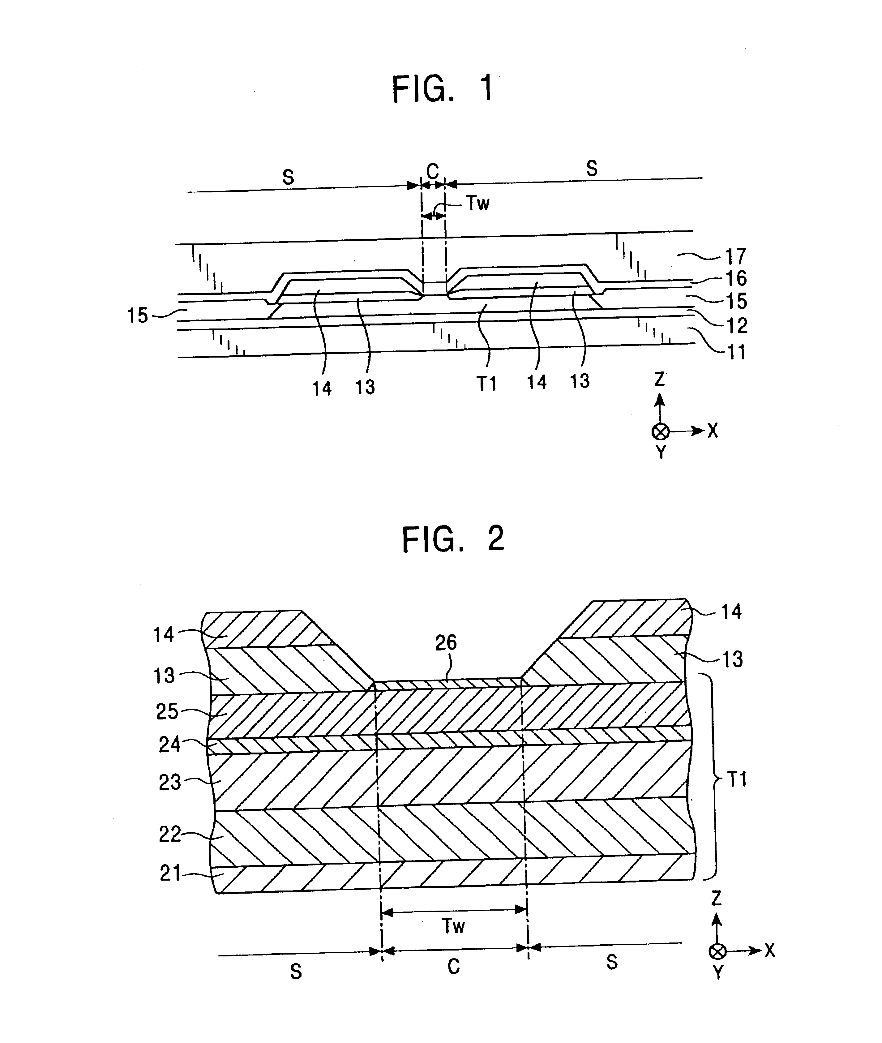
FIG. 1 is a partial front view of a magnetic sensing element according to a first embodiment of the present invention when viewed from a face that opposes a recording medium (hereinafter, the opposing face).
The magnetic sensing element shown in FIG. 1 is a magnetoresistive (MR) head for reading an external signal recorded on a recording medium. The opposing face is perpendicular to the surfaces of the layers that constitute the magnetic sensing element and is parallel to the magnetization direction of the free magnetic layer of the magnetic sensing element when no external magnetic field is applied. In FIG. 1, the opposing face is a flat plane parallel to the X-Z plane.
If the magnetic sensing element is applied to a floating magnetic head, the opposing face constitutes the air-bearing surface (ABS).
The magnetic sensing element is, for example, formed on a trailing end face of a slider composed of alumina titanium carbide (Al2O3—TiC). The slider is bonded on a elastic supporting memb...
second embodiment
FIG. 5 is a partial front view of a magnetic sensing element according to a second embodiment of the present invention when viewed from a face that opposes a recording medium (hereinafter, the opposing face).
As in the magnetic sensing element of the first embodiment shown in FIG. 1, the magnetic sensing element shown in FIG. 5 includes a lower shield layer 11 formed on a base layer (not shown), which is formed on a substrate (also not shown) and composed of an insulating material such as alumina. A lower gap layer 12 is formed on the lower shield layer 11, and a laminate T2 is disposed on the lower gap layer 12. The laminate T2 is formed by stacking a first antiferromagnetic layer, a pinned magnetic layer, a nonmagnetic material layer, and a free magnetic layer.
A pair of second antiferromagnetic layers 31 is formed on a top face T2a of the laminate T2, i.e., on the free magnetic layer. The second antiferromagnetic layers 31 are separated from each other in the track width direction,...
third embodiment
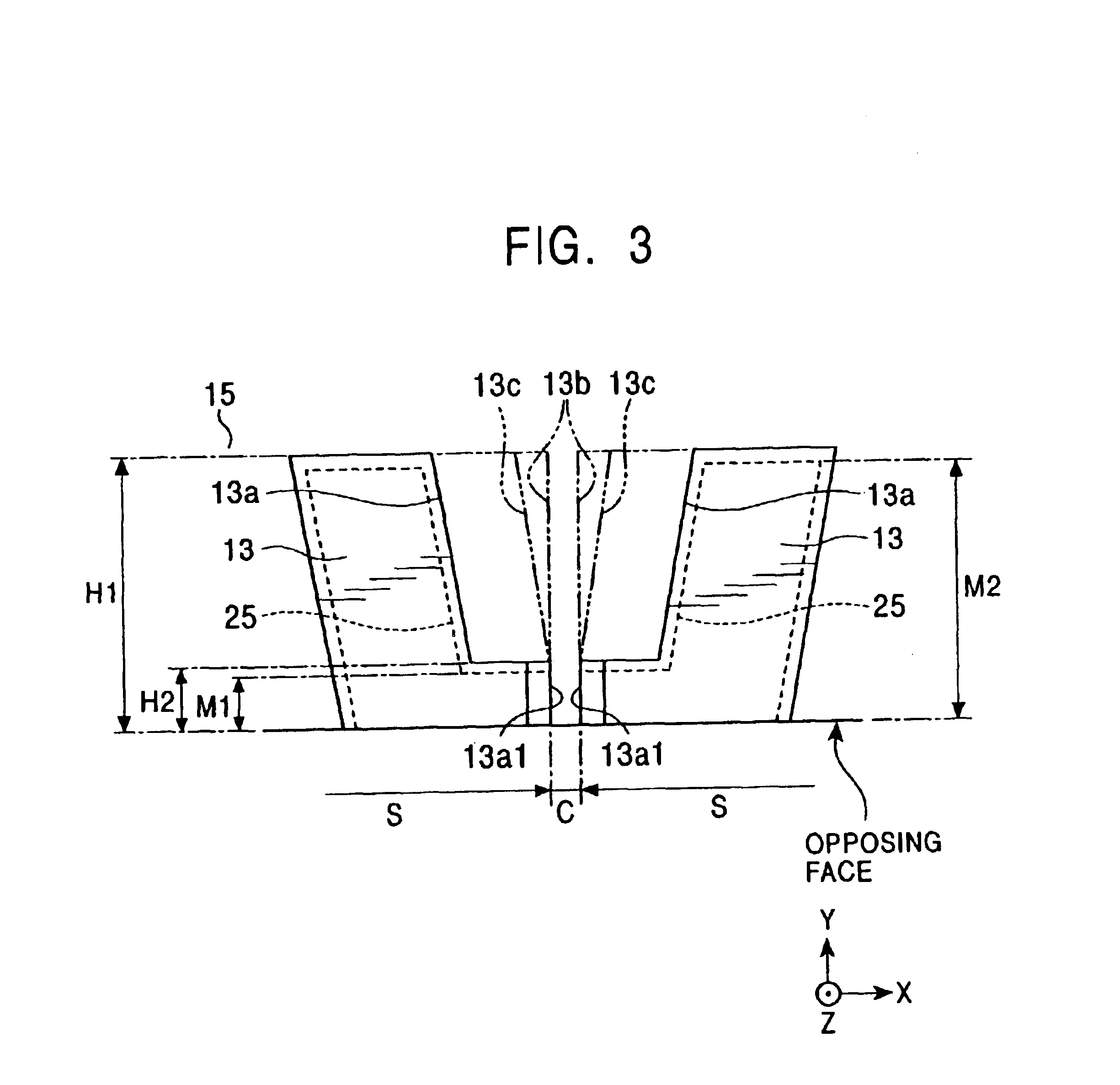
FIG. 8 is a partial enlarged view of a magnetic sensing element according to a third embodiment of the present invention showing a laminate T3, second antiferromagnetic layers 42, and electrode layers 43 near a track width region C.
Referring to FIG. 8, the laminate T3 is constituted from a base layer 51; a first antiferromagnetic layer 52; a pinned magnetic layer 56 of a synthetic ferri-pinned type constituted from a first pinned magnetic sublayer 53, a nonmagnetic interlayer 54, and a second pinned magnetic sublayer 55; a nonmagnetic material layer 57; a free magnetic layer 61 of a synthetic ferri-pinned type constituted from a second free magnetic sublayer 58, a nonmagnetic interlayer 59, and a first free magnetic sublayer 60; a pair of ferromagnetic layers 62 opposing each other with a gap corresponding to the track width therebetween, the ferromagnetic layers 62 being disposed on the first free magnetic sublayer 60; and a protective layer 63.
The base layer 51, the nonmagnetic ma...
PUM
| Property | Measurement | Unit |
|---|---|---|
| length | aaaaa | aaaaa |
| length | aaaaa | aaaaa |
| height | aaaaa | aaaaa |
Abstract
Description
Claims
Application Information
 - R&D
- Intellectual Property
- Life Sciences
- Materials
- Tech Scout
- Unparalleled Data Quality
- Higher Quality Content
- 60% Fewer Hallucinations
Browse by: Latest US Patents, China's latest patents, Technical Efficacy Thesaurus, Application Domain, Technology Topic, Popular Technical Reports.
© 2025 PatSnap. All rights reserved.Legal|Privacy policy|Modern Slavery Act Transparency Statement|Sitemap|About US| Contact US: help@patsnap.com