
Solder cracking resistant I/O pin connections

a technology of i/o pins and cracking resistance, applied in the field of i/o connections, can solve the problems of pin structure being particularly subject to problems, electrical connection quality may be compromised in some manner, and many applications for complex electronic devices involve particularly severe environmental conditions

Inactive Publication Date: 2001-01-09
LOCKHEED MARTIN CORP
View PDF7 Cites 12 Cited by
  • Summary
  • Abstract
  • Description
  • Claims
  • Application Information

AI Technical Summary

Benefits of technology

It is another object of the invention to provide a reliable solder connection suitable for low pin protrusion and header profile height and which is simple, inexpensive and readily assembled without specialized or complex tooling or machinery.
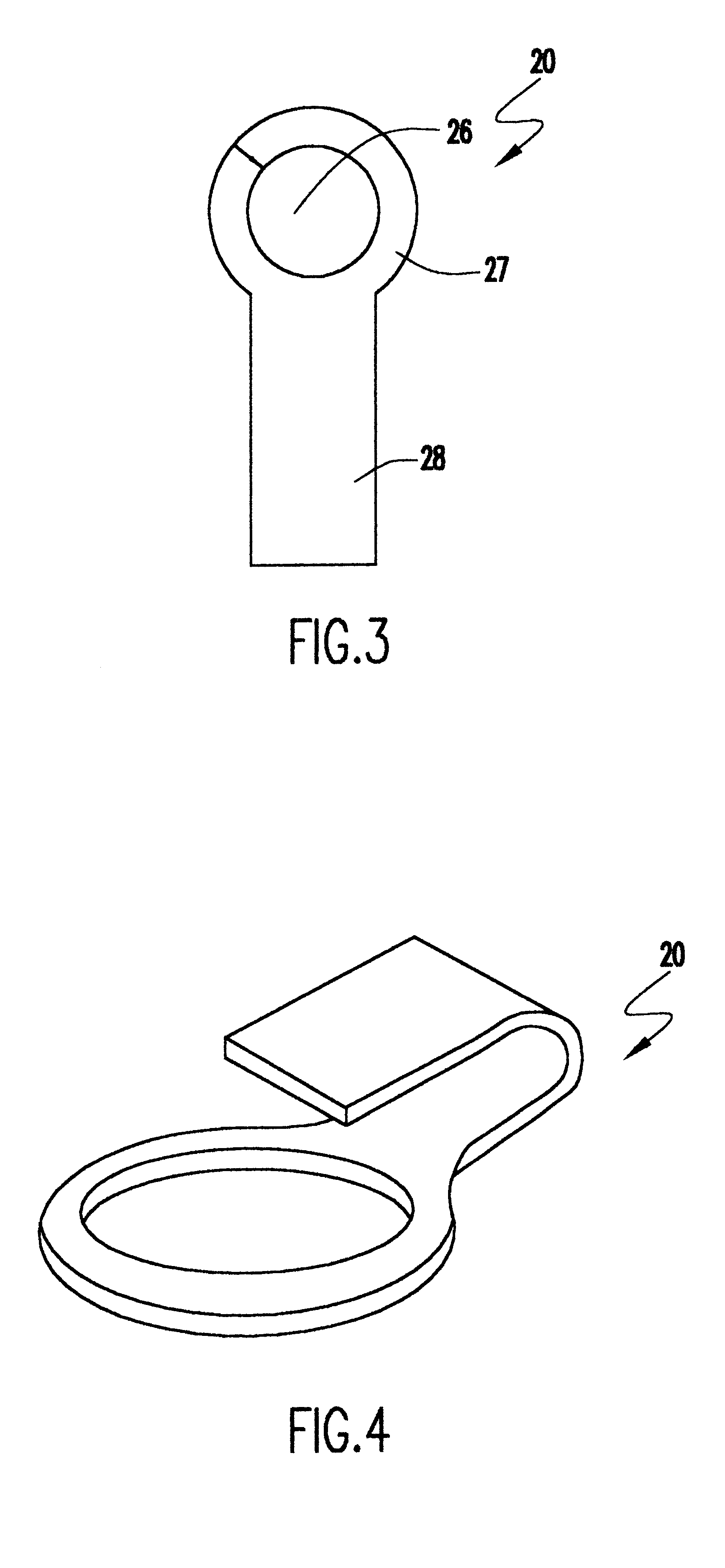
In order to accomplish these and other objects of the invention, a connection from a connection pad metallization to a pin is provided comprising a conductive strap including an aperture sized in accordance with the pin and connected to the connection pad and an end remote from the aperture connected to an end of the pin. The connection strap may be bonded to the connection pad and to the pin by solder bonds which, by virtue of the connection strap, are substantially isolated from stresses from and movement of the pin so that cracking of the solder bonds is avoided.

Problems solved by technology

In recent years, many applications for complex electronic devices have involved particularly severe environmental circumstances.
When the structures which support a component or module also make electrical connections thereto, the quality of the electrical connection may be compromised in some manner.
Pin structures are particularly subject to problems of this type since they, in essence, constitute cantilevered structures which can concentrate forces at the base or other support of the pin.
In particular, flexure of pin connections which are electrically attached to a circuit substrate by soldering tends to cause cracking of the solder connection even when the pin is otherwise supported by the substrate and / or a reinforcing header to which the circuit substrate may be attached.
Cracking of solder joints is particularly critical in regard to reliability of electrical apparatus since it is a progressive process which increases resistance and the potential for heating within the connection and, in severe cases could result in solder reflow including the formation of voids.
Further, electrical conduction across a crack may be possible under test conditions but may result in intermittent connection or disconnection when the electronic device is placed in service, engendering noise and other signal anomalies.
For example, welding, brazing and ultrasonic bonding are known but are expensive, generally inconvenient and require significantly more costly specialized equipment to perform.
Such equipment generally is of limited throughput and can significantly reduce manufacturing productivity.
However, this structure requires substantial pin height above the metallization of the circuit board whereas very low (e.g. 0.020 inches) pin protrusion is characteristic of modern modular circuit designs.
(The same is true of U.S. Pat. No. 5,389,743 for increasing connection security but does not provide for pin mounting.)
Low pin protrusion or header profile height as well as miniaturization of circuit modules limits the space and length available to accommodate pin flexure.
Accordingly, it is seen that known arrangements for improving reliability of electrical connections are not readily applicable to low pin protrusion height which is desirable in modern modular circuits.
Likewise, known arrangements are not generally simple or inexpensive and cannot be easily implemented in a modular circuit by solder bonding processes.

Method used


Image

  • Solder cracking resistant I/O pin connections
  • Solder cracking resistant I/O pin connections
  • Solder cracking resistant I/O pin connections

Examples


Embodiment Construction

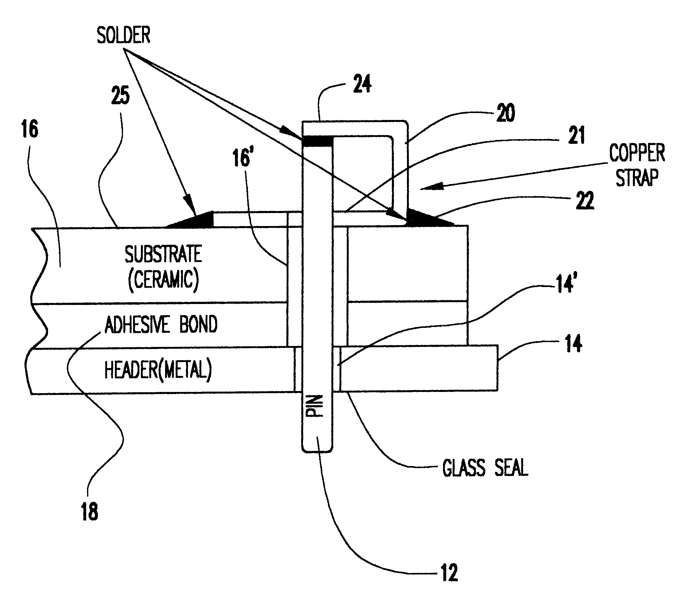
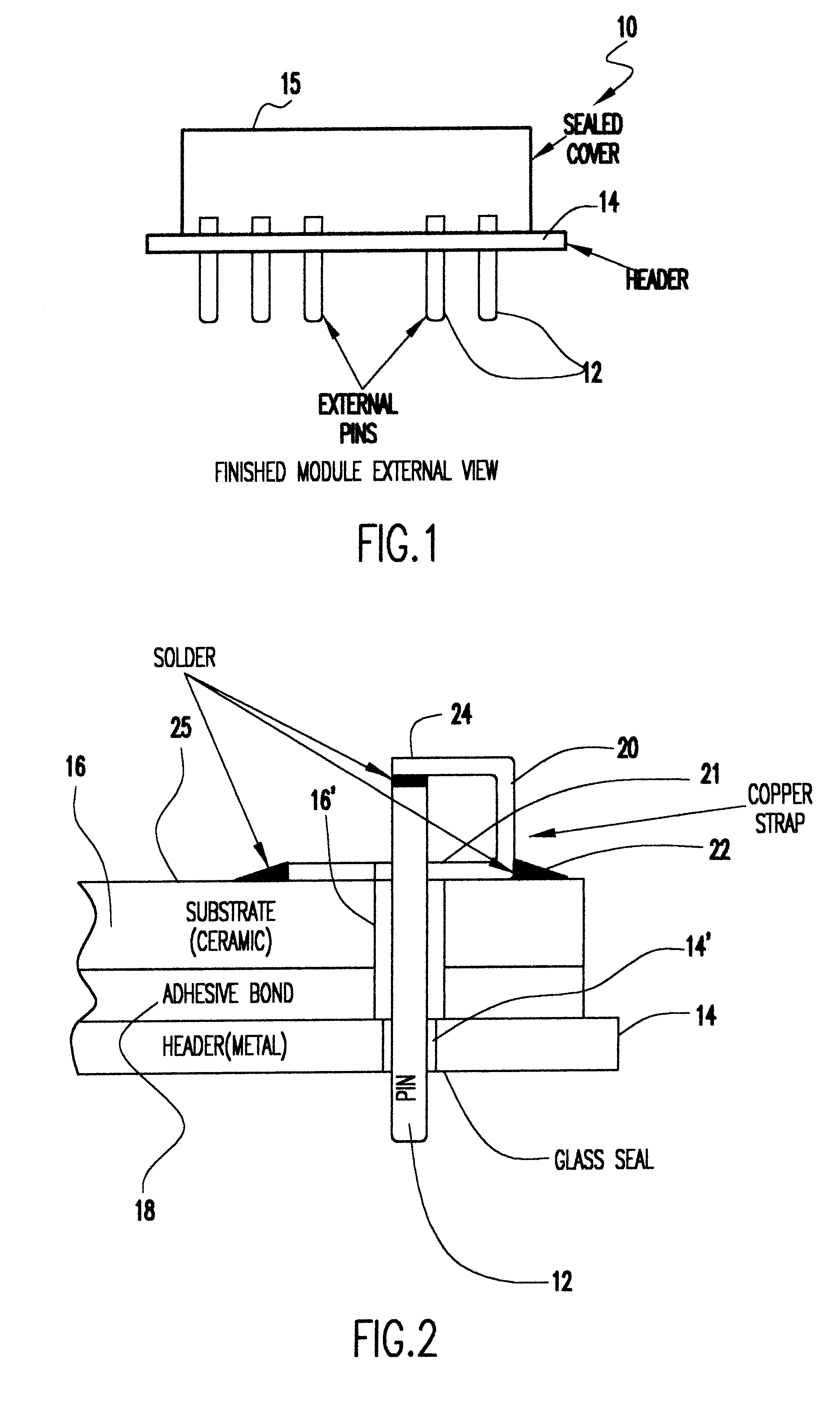
Referring now to the drawings, and more particularly to FIG. 1, there is shown a side view of the exterior of an exemplary circuit module 10 to which the invention may be applied. The circuit module includes a plurality of connection pins 12 which protrude below a header 14 that provides mechanical support for the pins. Generally, the header 14 is in the form of a metal plate, including glass seals 14' (FIG. 2) to insulate the pins therefrom and to seal the module, to enhance heat transfer but neither the form nor the material are critical to the practice of the invention. A cover 15 is sealed to the top side of the header 14 for hermetically sealing the components included in the module from the environment.

A portion of the internal structure of module 10 adjacent an arbitrary pin 12 is shown in cross-section in FIG. 2. The internal circuitry of the module, including surface metallization schematically indicated at 25, is carried by substrate 16 which is preferably formed of a cera...


PUM


Abstract

A robust connection is made from contact pad metallization on a substrate of a modular circuit to a connection pin by solder bonding. The connection includes a flexible copper strap with an aperture at one end which is sized to fit over the connection pin. The opposite end of the strap is solder bonded to an end of the connection pin. The connection thus made avoids application of stress from pin flexure to the solder bonds to avoid cracking while providing a connection having a low profile and minimal protrusion above the modular circuit substrate.

Description

1. Field of the InventionThe present invention generally relates to I / O connections (including power connections) of circuit modules and, more particularly, to improved connections to I / O pins in modular circuits which are subject to mechanical and thermal stressing.2. Description of the Prior ArtModular circuit designs have been known and employed in complex electronic devices for numerous applications. Modular circuit designs allow substantial convenience in packaging and manufacture as well as for repair and implementation of upgraded or improved modules which may improve the function of the overall apparatus as the improved modules become available. However, to allow realization of such advantages by modular construction of electronic apparatus, inputs and outputs, including power connections, must be made by a more-or-less readily detachable mechanical connections.In recent years, many applications for complex electronic devices have involved particularly severe environmental c...

Claims


Application Information

Patent Timeline
Patent Type & Authority Patents(United States)
IPC IPC(8): H01R4/02H05K3/30H01R12/04
CPCH01R4/023H05K3/308
Inventor DOWNEY, KAREN A.
Owner LOCKHEED MARTIN CORP
Learn More