
Resist Composition

a composition and resist technology, applied in the field of resist composition, can solve the problems of reducing throughput, obstructing the full implementation of this technique in the semiconductor industry, and current photoresist technologies suffer from the “trade-off” between resolution and exposure speed/sensitivity, so as to achieve good balance between resolution and sensitivity, reduce scattering, and improve exposure control

Pending Publication Date: 2022-06-09
UNIV OF MANCHESTER
View PDF0 Cites 0 Cited by
  • Summary
  • Abstract
  • Description
  • Claims
  • Application Information

AI Technical Summary

Benefits of technology

[0018]According to a first aspect of the present invention there is provided a resist composition comprising an anti-scattering component and a resist component. The anti-scattering component suitably serves to reduce scattering (of either or both primary / incident radiation and / or secondary radiation) to thereby provide better exposure control and minimize proximity effects. The resist component suitably imparts resist qualities to the composition whereby the “developer-solubility” of (wavelength / radiation-appropriate) radiation-exposed portions of the composition (or coating thereof) is selectively transformed in contrast to unexposed portions, so that exposed and unexposed portions exhibit differential developer solubility. The anti-scattering component and resist component may be separate compounds, or may be mutually associated or somehow connected, whether chemically and / or physically, suitably by way of bonding. Such an association can facilitate interplay or collaboration between exposure control and sensitivity control functions for the benefit of each, thereby affording a resist composition that produces good resolution alongside good sensitivity.
[0071]According to a further aspect of the invention, there is provided an integrated circuit wafer comprising a plurality of integrated circuit dice, the integrated circuit wafer being obtainable by, obtained by, or directly obtained by a method of fabricating an integrated circuit wafer as defined herein. Such integrated circuits and wafers have a very high resistance, a high dry etch selectivity (typically above 20:1—i.e. the resist etches slower than the underlying silicon substrate by a factor of 20 or more). This in turn affords high aspect ratios.

Problems solved by technology

Recent developments in extreme ultraviolet (EUV) lithography, at 13.5 nm, has enabled some further scaling / miniaturization of integrated circuits, but enormous challenges still obstruct the full implementation of this technique in the semiconductor industry.
Unfortunately, these resist materials require longer patterning times, resulting in reduced throughput.
However, current photoresist technologies suffer from the “trade-off” between resolution and exposure speed / sensitivity (i.e. throughput).
Though better exposure control is afforded with shorter UV-wavelengths, which tend to afford higher resolution photolithographic patterns (due to their ability to interact with features on a smaller scale), such short UV wavelengths are generally better absorbed (by photoresists) than longer wavelengths due to the greater prevalence of spin-allowed electronic transitions (within absorbing molecules and atoms) at shorter wavelengths, thereby limiting the supply of usable energy.
Since such absorption events tend to “lock-up” a photon's energy, since eventual vibronic energy dissipation is usually fruitless from a photolithography perspective, the energy of these photons can no longer be harnessed in a photolithographically-fruitful manner (e.g. through triggering chemical reactions that selectively modify the solubility of exposed vs non-exposed portions of a photoresist by promoting appropriate bond formations or bond scissions, depending on the tone of the resist).
As such, resolution gains are typically at the expense of photolithographic kinetics.
Though photonic energy is absorbed during this ionization process, the energy (or at least a part thereof) is fruitfully released (rather than fruitlessly trapped) for further exposure events, though naturally this can in turn lead to exposure control problems, especially in view of the angle at which the electrons are ejected (˜80° C.) which leads to proximity effects.
The reliance on post-exposure acid diffusion (usually during post-exposure bakes) for successful exposures / developments can be somewhat limiting, especially in terms of the resolution and contrast of the resulting pattern.

Method used


Image

  • Resist Composition
  • Resist Composition
  • Resist Composition

Examples


example 1

on of Anti-Scattering Compounds

[0622]In general, a resist composition of the invention (e.g. photoresist) may be produced by forming a composition that includes an anti-scattering compound as defined herein. Suitably the composition also comprises a coating solvent to enable the anti-scattering compound to be applied as a resist coating.

[0623]Since the anti-scattering compound suitably includes a low-density, high molecular weight polymetallic cage (since such structures produce less scattering owing to the amount of empty space within such cage structures), any polymetallic cage may be used to obtain the relevant beneficial effect. By way of guidance to the skilled person, suitable structures may include any polymetallic cage complexes the same or similar to those disclosed in G. F. S. Whitehead, F. Moro, G. A. Timco, W. Wernsdorfer, S. J. Teat and R. E. P. Winpenny, “A Ring of Rings and Other Multicomponent Assemblies of Clusters”, Angew. Chem. Int. Ed., 2013, 52, 9932-9935. This ...

example 2

on of Resist Compositions

[0632]The anti-scattering compounds of Examples 1A and 1B may be considered antiscattering-resist hybrid compounds, since they incorporate both an anti-scattering component (i.e. the overall low-density metal cage compound) and resist components (i.e. 2-Methyl-4-pentenoate resist ligands which bear terminal alkene groups which are cross-linkable).

[0633]As such, various resist compositions were formed and tested for effectiveness.

Cr7Ni base structure (see FIG. 13)

Example 2A(i) and (ii)—Formulation A (Cr7Ni / 2-Methyl-4-pentenoate Complex+Sulfoniumtriflate)

[0634]Formulations A(i) and (ii) were prepared using the antiscattering-resist hybrid compound of Example 1A, one without the Tris(4-tert-butylphenyl)sulfoniumtriflate (A(i)) and another with the Tris(4-tert-butylphenyl)sulfoniumtriflate (A(ii)).

[0635]To form the resist composition, 20 mg antiscattering-resist hybrid compound of Example 1A is dissolved in 1 g of tert butyl methyl ether (MTBE) and filtered thr...

example 3

on of Resist-Coated Substrates

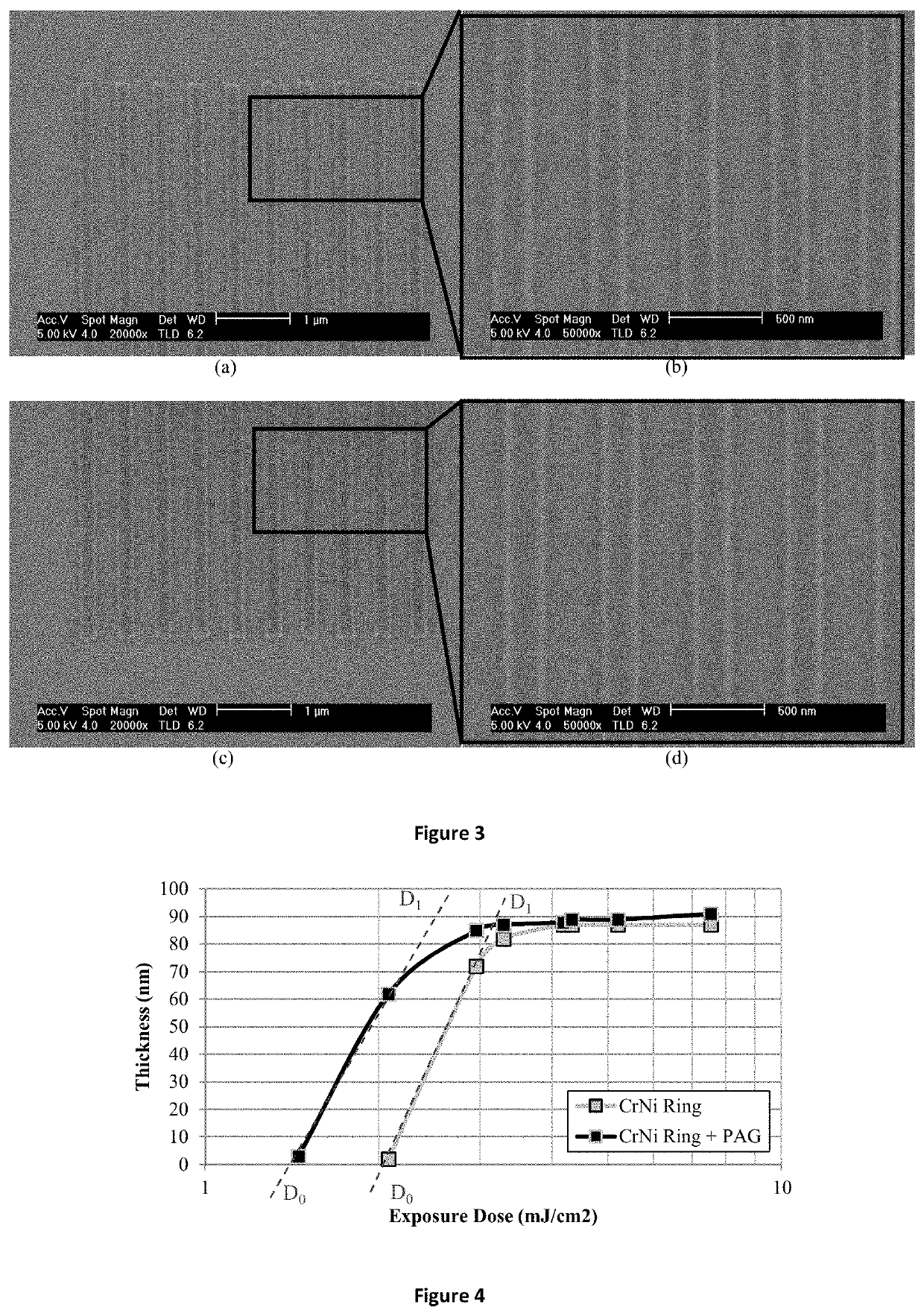
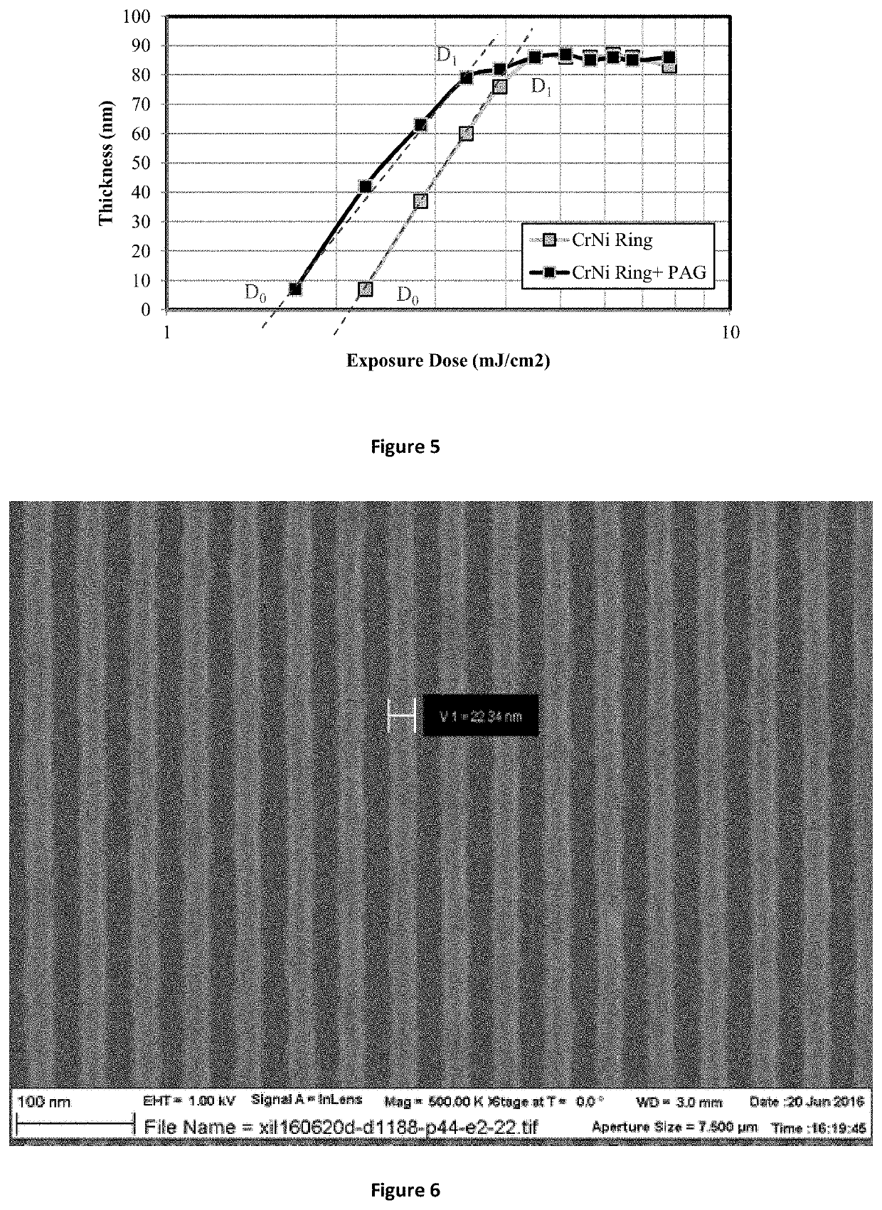
[0651]Each of the aforementioned Example resist compositions 2A-2H were spun onto 10 mm×10 mm silicon substrates. Each resist composition was spun using a spin cycle of 8000 rpm for 60 seconds, which was followed by a soft-bake at 100° C. for 2 minutes, allowing the cast solvent to evaporate. The resist film resulted with a thickness of 100 nm. The resist films were exposed with 248 and 193 nm radiation through a Silver optical mask which consisted of 250 and 200 nm features. Each material was developed using a solution of Hexane, for 30 s followed by an N2 blow dry.

Results and Discussion

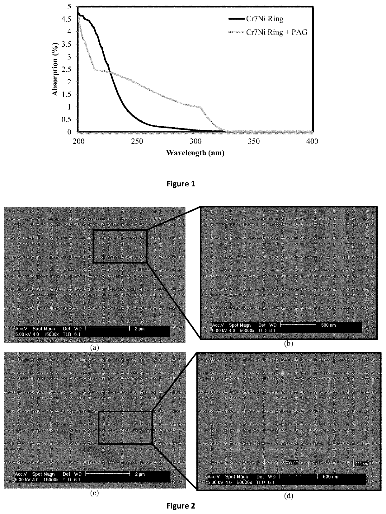
[0652]FIG. 1 shows a graph illustrating how radiation-absorption varies with incident wavelength for each of Formulations A(i) (i.e. Cr7Ni metal complex only) and Formulation A(ii) (Cr7Ni complex+photoacid generator).

[0653]It is evident from FIG. 1 that, at a wavelength of 248 nm (suitable for photolithography), the Cr7Ni ring molecule alone absorbs approximately 0.5% o...


PUM

PropertyMeasurementUnit
densityaaaaaaaaaa
densityaaaaaaaaaa
atomic numberaaaaaaaaaa

Abstract

The present invention relates to resist compostions, in particular to photoresists that can be used in photolithography, especially in the fabrication of integrated circuits and derivative products. The resist compositions of the invention include an anti-scattering component which has a significant amount of empty space, and thus fewer scattering centers, such that radiation-scattering events are more limited during exposure. Such anti-scattering effects can lead to improved resolutions by reducing the usual proximity effects associated with lithographic techniques, allowing the production of smaller, higher resolution microchips. Furthermore, certain embodiments involve anti-scattering components which are directly linked to the resist components, which can improve the overall lithographic chemistry to provide benefits both in terms of resolution and resist sensitivity.

Description

INTRODUCTION[0001]The present invention relates to a resist composition, in particular to a photoresist composition. The present invention also relates to methods of preparing and using such resist compositions, alongside a variety of related aspects.BACKGROUND[0002]There is a continuous drive in the electronics industry to miniaturize integrated circuits (ICs), for a variety of reasons well known to those skilled in the art. Significant developments in the semiconductor industry were made possible by advances in photolithography, from the micron scale to the nanometer scale, but the physical resolution limits of optical lithography have now almost been reached, thus constraining further advancement. However, continued growth of the semiconductor industry depends on increasing the performance of integrated circuits on a silicon substrate.[0003]Recent developments in extreme ultraviolet (EUV) lithography, at 13.5 nm, has enabled some further scaling / miniaturization of integrated circ...

Claims


Application Information

Patent Timeline
Patent Type & Authority Applications(United States)
IPC IPC(8): G03F7/20G03F7/004G03F7/031G03F7/038G03F7/16G03F7/32H01L21/027H01L21/56H01L21/768H01L21/78
CPCG03F7/2061G03F7/0042G03F7/031G03F7/038G03F7/162G03F7/168H01L24/03G03F7/325H01L21/0274H01L21/56H01L21/76895H01L21/78G03F7/2002G03F7/004G03F7/20G03F7/2059H05K3/303
Inventor LEWIS, SCOTTWINPENNY, RICHARDYEATES, STEPHENFERNANDEZ, ANTONIO
Owner UNIV OF MANCHESTER
Learn More